Introduction
Printed circuit board (PCB) layout serves as the foundation for reliable electronic systems, directly influencing signal integrity, thermal performance, and manufacturability. Engineers often encounter PCB layout errors that lead to costly redesigns, field failures, or performance degradation in applications from consumer devices to industrial controls. These common PCB design mistakes stem from overlooking fundamental principles during the layout phase, such as trace routing, component placement, and layer management. A thorough PCB layout checklist and design review process can mitigate these issues, ensuring compliance with industry expectations. This article outlines the top 10 PCB layout errors, explaining their causes, impacts, and practical avoidance strategies. By mastering these, electrical engineers can enhance product reliability and reduce iteration cycles.
1. Improper Component Placement
Component placement errors rank among the most frequent PCB layout errors, often resulting from prioritizing aesthetics over functionality. Placing high-speed signals near noisy power components induces crosstalk and electromagnetic interference, compromising signal quality. Similarly, decoupling capacitors positioned too far from integrated circuits fail to provide effective noise suppression. Thermal hotspots emerge when heat-generating parts cluster without adequate spacing, accelerating material degradation. To avoid this, start with a logical grouping: analog, digital, and power sections separated by ground planes. Perform iterative simulations early, adjusting placements to minimize trace lengths for critical signals.
Follow a structured PCB layout checklist that includes signal flow analysis from schematic to board. Allocate sufficient clearance around connectors and mounting holes to prevent mechanical stress during assembly. Verify thermal dissipation paths by estimating junction temperatures based on power dissipation ratings. This approach aligns with standard design practices, fostering robust layouts.
2. Inadequate Trace Width and Spacing
Undersized traces represent a classic among common PCB design mistakes, leading to excessive resistance, voltage drops, and overheating under load. Narrow traces for high-current paths violate current-carrying capacity guidelines, risking electromigration over time. Insufficient spacing between traces invites short circuits during manufacturing or arcing in high-voltage designs. Engineers must calculate trace widths using factors like copper thickness, ambient temperature, and allowable temperature rise. Standard formulas account for these variables to ensure safe operation.
In multilayer boards, inner layer traces demand even greater attention due to poorer heat dissipation. Implement design rules that enforce minimum spacing scaled to voltage levels and manufacturing tolerances. During PCB design review, cross-check calculations against layer stackup specifics. This prevents failures in power distribution networks and maintains signal fidelity.
3. Poor Ground Plane Utilization
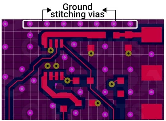
Neglecting continuous ground planes creates high-impedance return paths, amplifying noise and ground bounce in mixed-signal designs. Split planes without stitching vias force currents to detour, increasing inductance and EMI susceptibility. Common PCB layout errors here include isolating digital and analog grounds improperly, leading to loops that couple noise across sections. A solid ground plane under high-speed signals provides low-inductance returns, essential for impedance control.
To avoid this, pour full ground planes on inner layers, using vias liberally at plane transitions. Stitch split planes with arrays of vias spaced at a fraction of the wavelength of highest frequencies. Verify plane integrity in the layout tool by checking for voids larger than allowed by design rules. This strategy minimizes loop areas and enhances overall EMC performance.
4. Ignoring Signal Integrity Issues
Signal integrity problems, such as reflections and crosstalk, arise from mismatched impedances and excessive trace lengths in high-speed layouts. Uncontrolled rise times on long traces cause overshoot and ringing, potentially damaging components. PCB layout errors like sharp bends or stubs exacerbate these effects by introducing discontinuities. Engineers should target controlled impedance for critical nets, typically 50 ohms single-ended or 100 ohms differential.
Use length-matching for clock and data lines to prevent skew. Simulate pre-layout with tools that model transmission line behavior, adjusting widths and spacing accordingly. Post-layout verification confirms timing margins. Adhering to these steps ensures data eyes remain open across operating conditions.
5. Inadequate Thermal Management
Overlooking thermal vias and copper pours leads to hotspots that exceed component ratings, causing derating or failure. High-power devices like voltage regulators demand direct heat paths to planes, yet common PCB design mistakes place them without support. Junction-to-ambient thermal resistance spikes in dense layouts, reducing lifespan. Calculate power budgets early and model heat flow using finite element approximations.
Incorporate thermal reliefs on pads and vias under hot components to balance solderability and dissipation. Space heat sources to leverage natural convection, and consider board thickness for rigidity. During design review, inspect for uniform dissipation across the board. Per IPC-2221 guidelines, these practices sustain performance under load.
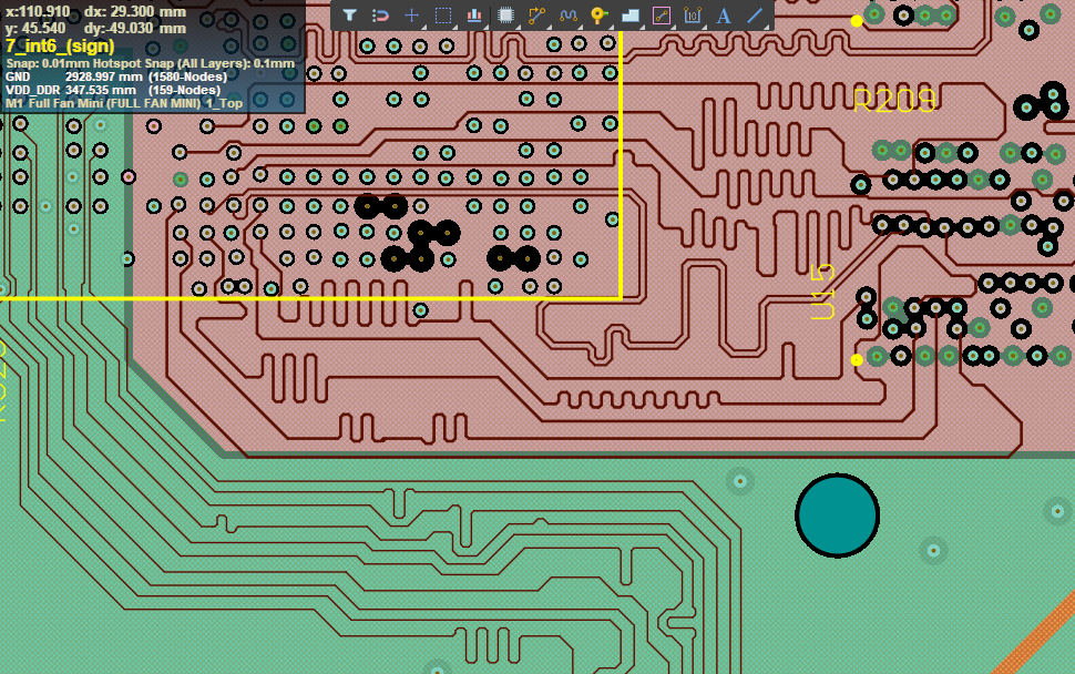
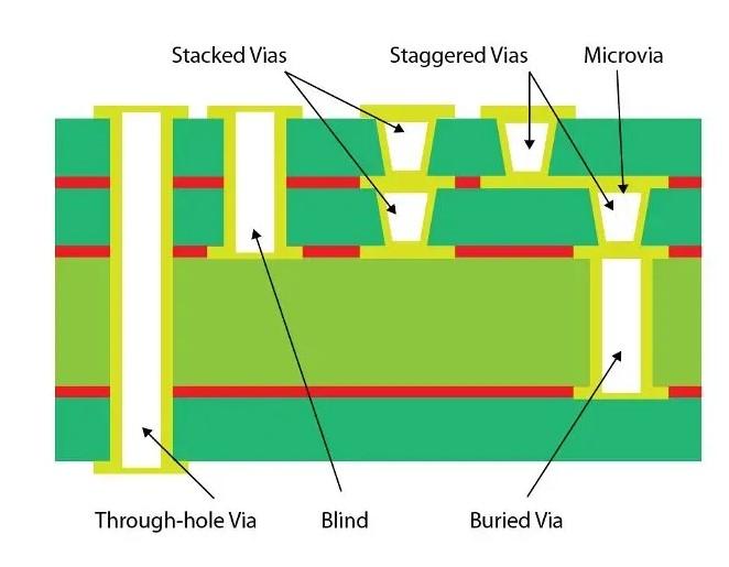
6. Excessive or Improper Via Usage
Vias introduce parasitic inductance and capacitance, degrading high-frequency signals if overused or poorly placed. Blind or buried vias misused in simple designs inflate costs without benefit, a frequent PCB layout error. Clusters of vias under pins create solder voids during reflow. Limit via count by optimizing routing on available layers, using larger antipads for power vias to reduce impedance.
Prefer microvias for dense BGAs, ensuring fanout patterns comply with land pattern standards. Check via current capacity against trace equivalents, adding reliefs where needed. A PCB layout checklist should flag excessive via densities exceeding drill feasibility.
7. Faulty Layer Stackup Design
Incorrect layer stackup causes asymmetric fields, warping, and poor impedance control. Common mistakes include alternating signal and plane layers haphazardly, leading to crosstalk between adjacent signals. Thin dielectrics without matching prepregs result in impedance mismatches across the board. Define stackup based on routing density, speed requirements, and mechanical constraints like board thickness.
Symmetrical builds prevent warpage during fabrication and reflow. Simulate impedance profiles for each layer, targeting uniformity within 10%. Consult fabricator input early for material CTE matching. This foundational step avoids downstream PCB layout errors.
8. Power Distribution Network Flaws
Decoupling strategy failures manifest as voltage ripple on power rails, starving ICs during transients. Insufficient bulk capacitance or poor placement amplifies PDN impedance peaks. PCB design mistakes here skip plane capacitance benefits, relying solely on discrete caps. Model PDN impedance targets below milliohms at target frequencies.
Distribute caps hierarchically: local to pins, then board-level. Use power planes for low inductance, with decoupling arrays tuned to switching harmonics. Verify in simulation by injecting current steps and checking ripple.
9. Neglecting Manufacturability Rules
Failing design for manufacturability (DFM) leads to yield losses from narrow clearances or unsupported features. Trace-to-pad spacing too tight causes solder bridging, a prevalent PCB layout error. Ignoring panelization rules complicates production runs. Enforce DRCs for etch factor, annular ring, and minimum feature sizes per fabricator capabilities.
Review silkscreen legibility and solder mask expansion to prevent exposure. Test netlist integrity against schematic. IPC-A-600 criteria guide acceptability inspections, ensuring high yields.
10. Skipping Comprehensive Design Review
Rushing without peer review perpetuates subtle errors like netlist discrepancies or DRC waivers. Isolated design work misses systemic issues like timing violations. A formal PCB design review process catches these before fabrication. Checklist items cover schematic capture fidelity, signal integrity sims, thermal analysis, and DFM.
Involve cross-functional teams for blind spots. Document waivers with rationale and mitigations. Iterative reviews refine layouts iteratively.
Conclusion
Mastering PCB layout demands vigilance against these top 10 common mistakes, from placement to review. Implementing a rigorous PCB layout checklist integrates signal integrity, thermal, and DFM considerations upfront. Electrical engineers benefit from structured approaches that reference standards like IPC-2221 for design guidelines. Proactive avoidance strategies yield reliable, cost-effective boards. Regular design reviews cement these habits, elevating project success rates.
FAQs
Q1: What are the most critical PCB layout errors for high-speed designs?
A1: High-speed PCB layout errors include impedance mismatches, poor return paths, and length skews, which degrade eye diagrams. Prioritize controlled impedance traces, solid ground planes, and length tuning in your PCB layout checklist. Simulate pre- and post-layout to verify margins. This structured review prevents data errors in gigabit applications.
Q2: How can I create an effective PCB design review process?
A2: Start with a PCB design review checklist covering DRC compliance, signal integrity, thermal sims, and DFM. Involve schematic, layout, and manufacturing experts for diverse insights. Use checklists to flag common PCB design mistakes like via overuse. Document findings and iterate before tape-out.
Q3: What role do standards play in avoiding PCB layout errors?
A3: Standards like IPC-2221 provide guidelines for trace sizing and spacing, reducing common PCB design mistakes. They ensure consistency in thermal management and layer stackup. Integrate them into your workflow for reliable outcomes. Reference during design review for compliance.
Q4: Why is ground plane design a frequent PCB layout error?
A4: Incomplete ground planes create inductive loops, coupling noise to signals. Avoid by pouring full planes and stitching splits with vias. This lowers PDN impedance per best practices. Verify in layout tools during PCB design review.
References
IPC-2221B — Generic Standard on Printed Board Design. IPC, 2012
IPC-A-600K — Acceptability of Printed Boards. IPC, 2020


