Introduction
In modern electronics, effective power distribution is essential for reliable circuit performance, especially as devices operate at higher speeds and densities. PCB PDN design forms the backbone of this process, ensuring stable voltage delivery to components while minimizing noise and voltage droop. Achieving low impedance across a wide frequency range prevents issues like signal degradation and electromagnetic interference. This guide explores the fundamentals and best practices for low-impedance PDN design, tailored for electric engineers seeking structured approaches to power integrity. By focusing on power planes, decoupling strategies, and simulation techniques, engineers can optimize their layouts for demanding applications. Key elements include maintaining target impedance profiles and addressing high-frequency behaviors inherent in contemporary PCB designs.
Understanding PCB PDN Design and Its Importance
The power distribution network in a PCB encompasses all conductive paths from voltage regulators to load components, including planes, traces, vias, and capacitors. PCB PDN design aims to provide a low-impedance path for both DC current and transient high-frequency currents generated by switching ICs. Poor PDN performance leads to voltage fluctuations that couple into signals, causing timing errors, jitter, or outright failures in high-speed systems. Engineers must consider the entire network's impedance spectrum, from low frequencies dominated by bulk capacitance to high frequencies where package and board parasitics prevail. Adhering to established guidelines, such as those in IPC-2221C, ensures designs meet reliability thresholds for power delivery. Ultimately, robust PDN design directly impacts system margins, thermal management, and overall product yield.
Low impedance in the PDN translates to stable power rails under varying loads, critical for processors, FPGAs, and memory interfaces. Impedance peaks, often from resonances between planes or inadequate decoupling, amplify noise and reduce noise margins. Electric engineers prioritize PDN early in the layout phase to avoid costly respins. Factors like board stackup, layer count, and material properties influence achievable impedance levels. By modeling the PDN as a distributed RLC network, designers can predict and mitigate vulnerabilities before fabrication.
Principles of Low-Impedance Power Planes
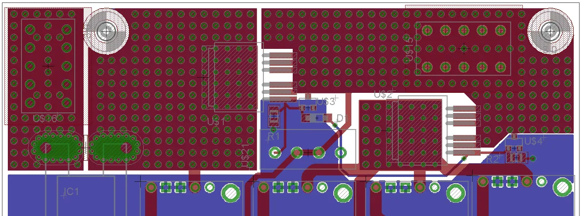
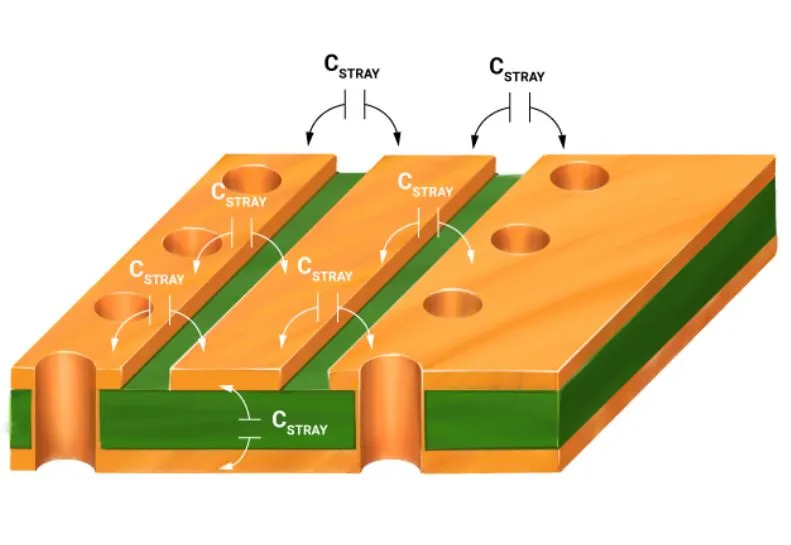
Low impedance power planes serve as the primary reservoir for charge in PCB PDN design, offering far lower inductance than traces due to their wide area. Solid, continuous planes minimize loop inductance by providing short return paths adjacent to signal traces. Engineers should pair power and ground planes closely in the stackup to enhance capacitive coupling, which suppresses high-frequency noise. Avoid splitting planes under active components to prevent current detours that increase effective impedance. IPC-2152 provides guidance on sizing conductors, including planes, to handle sustained currents without excessive heating.
Plane thickness and material selection further refine impedance characteristics. Thicker copper reduces DC resistance, while surface roughness affects high-frequency skin effect losses. Vias connecting planes must be densely placed to maintain low via inductance, especially in multi-layer boards. Engineers evaluate plane resonance frequencies, where parallel-plane modes can create impedance peaks around hundreds of MHz. Stitching vias along plane edges dampens these modes effectively. This structured approach ensures the power plane contributes minimally to overall PDN impedance.
Decoupling Capacitor Placement Strategies
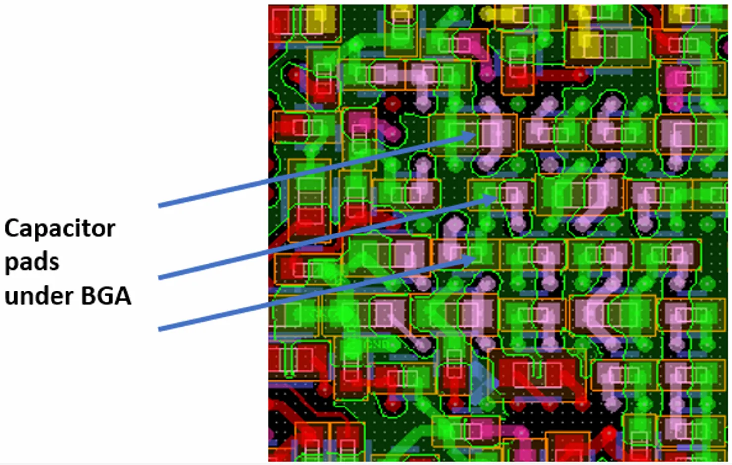
Decoupling capacitor placement is pivotal in PCB PDN design, bridging gaps in plane impedance at mid-to-high frequencies. Capacitors store charge locally, supplying transient currents faster than distant regulators. Place them as close as possible to IC power pins, ideally within millimeters, to minimize inductive loops formed by traces and vias. Use a mix of values: small ceramics for GHz range, larger ones for lower frequencies, ensuring broad coverage. Under-BGA placement on the opposite side requires short vias to maintain effectiveness.
Optimal strategies involve arraying capacitors around pin groups, with dedicated power-ground via pairs per cap. This reduces ESL and ESR contributions to impedance. J-STD-001J outlines soldering criteria to ensure reliable connections, preventing voids that degrade performance. Avoid routing signals between cap and pin to preserve low-inductance paths. Engineers verify placement through loop area minimization, targeting sub-nH inductance. These practices collectively flatten the PDN impedance curve.
Power Integrity Simulation Techniques
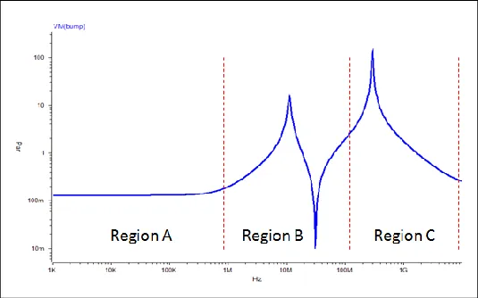
Power integrity simulation verifies PCB PDN design by modeling impedance versus frequency against a target profile. Start with a target impedance calculated from allowable ripple and maximum current, ensuring the simulated curve stays below it across the operational bandwidth. Tools extract S-parameters from layouts to build accurate 3D models including die, package, and board. Simulate transient responses to switching loads, identifying droop or overshoot.
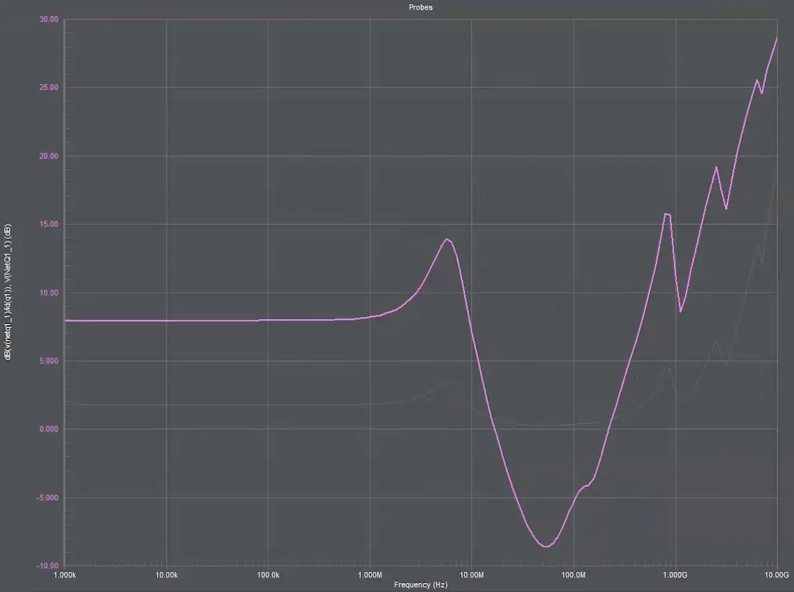
Frequency-domain analysis reveals resonances, guiding capacitor value tweaks or via additions. Time-domain checks validate voltage stability under real workloads. Iterate stackup and decoupling until margins are met. This simulation-first workflow reduces empirical fixes post-prototype. Electric engineers integrate PI early, correlating with measurements like VNA sweeps for validation.
High-Frequency PDN Design Considerations
High-frequency PDN design grapples with skin effect, where current crowds plane surfaces, elevating effective resistance above DC values. Cavity resonances between power-ground pairs emerge around f = c / (2 * spacing * sqrt(εr)), demanding targeted mitigation. Dense decoupling arrays counteract these peaks, while embedded capacitors in advanced stackups offer ultra-low ESL. Via transitions from package to board must use arrays to fan out currents evenly.
Signal return currents seek low-impedance paths, so co-locate power planes near noisy signals. Material dielectric constants influence propagation delays and coupling. Engineers employ cavity stitching and interplane capacitors for GHz+ operation. These techniques ensure low impedance power planes perform in high-speed environments like 5G or AI accelerators.
Conclusion
Mastering PCB power distribution through low-impedance design hinges on integrated strategies for planes, decoupling, and simulation. Electric engineers benefit from a systematic approach: define targets, model iteratively, and validate physically. Key takeaways include prioritizing plane integrity, precise capacitor placement, and PI analysis for robust performance. Adopting these practices aligns with industry benchmarks, yielding reliable, high-margin boards. As frequencies rise, proactive PDN optimization remains indispensable for next-generation electronics.
FAQs
Q1: What is the role of low impedance power planes in PCB PDN design?
A1: Low impedance power planes provide a low-inductance reservoir for DC and transient currents, minimizing voltage droop and noise. They pair with adjacent ground planes for inherent decoupling capacitance. Proper sizing per guidelines ensures thermal reliability. This foundation supports stable operation across frequencies, critical for high-speed ICs. Engineers focus on continuity and via density to achieve design goals.
Q2: How does decoupling capacitor placement affect power integrity simulation results?
A2: Decoupling capacitor placement directly influences PDN impedance profiles in simulations, with closer proximity reducing loop inductance and filling frequency gaps. Arrays near pins flatten curves below targets. Simulations reveal optimization needs, like value spreads. Poor placement spikes impedance, causing ripple. Engineers use this feedback for layout refinement.
Q3: Why is power integrity simulation essential for high-frequency PDN design?
A3: Power integrity simulation identifies resonances and droops in high-frequency PDN design before fabrication. It models parasitics accurately, guiding plane stitching and cap strategies. Target impedance compliance ensures noise margins. Without it, prototypes risk failure. Electric engineers rely on it for iterative, risk-reduced development.
Q4: What are common best practices for low impedance power plane implementation?
A4: Implement solid planes without splits under loads, use tight stackups, and add stitching vias. Follow conductor sizing rules for currents. Combine with decoupling for broadband coverage. Verify via PI tools. These steps yield effective low impedance power planes.
References
IPC-2221C — Generic Standard on Printed Board Design. IPC, 2023
IPC-2152 — Standard for Determining Current Carrying Capacity in Printed Board Design. IPC, 2009
J-STD-001J — Requirements for Soldered Electrical and Electronic Assemblies. IPC, 2024