Introduction
In modern PCB design, routing high-speed signals across multiple layers presents significant challenges related to signal integrity and electromagnetic interference. Via stitching emerges as a critical technique to address these issues by creating robust interconnections between ground and power planes. Electric engineers rely on via stitching to minimize inductance in return paths and ensure stable performance in dense layouts. This guide explores the principles, types, and best practices of PCB via stitching, including via fence configurations, to help designers achieve optimal results. Ground plane stitching and power plane stitching play pivotal roles in maintaining low-impedance connections throughout the board. Mastering these methods leads to reliable boards that meet demanding electrical requirements.
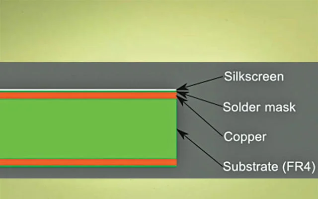
What Is PCB Via Stitching?
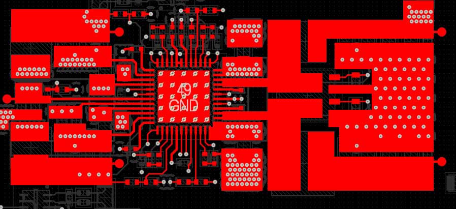
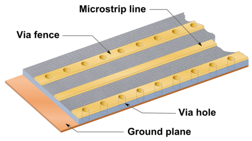
PCB via stitching involves placing multiple vias in a pattern to electrically connect adjacent copper planes, typically ground or power layers, across the board stackup. These vias act as parallel conductors that reduce the effective impedance of the plane-to-plane connection. Unlike isolated signal vias, stitching vias are redundant in routing but essential for structural integrity of the power distribution network. A via fence represents a specialized form where vias are arranged in a dense linear array, often along board edges or around sensitive areas. This technique prevents the formation of slots that could radiate electromagnetic interference. Engineers use via stitching routinely in multi-layer boards to bridge splits or gaps in planes.
Why Via Stitching Matters in PCB Design
Via stitching directly contributes to EMI reduction by providing low-inductance return paths for high-frequency currents. Without proper stitching, discontinuities in ground planes create slot antennas that couple noise to adjacent traces, degrading signal integrity. In high-speed designs, return currents follow the path of least impedance, and stitching ensures they remain confined to the reference plane. Power plane stitching similarly supports stable voltage delivery, preventing voltage droops under load. These practices enhance overall board reliability, especially in environments with stringent electromagnetic compatibility requirements. For electric engineers, neglecting via stitching often results in failed compliance tests or intermittent failures in prototypes.
Technical Principles Behind Via Stitching
The core principle of via stitching lies in minimizing loop inductance between planes. High-frequency currents seek the shortest return path, and plane splits force them to detour, increasing inductance and radiated emissions. Stitching vias parallelize the connection, effectively shorting the planes at multiple points and distributing current evenly. This reduces the equivalent series inductance, calculated as L_eq = L_via / N for N vias, where L_via is the inductance of a single via. In RF applications, via fence configurations create a Faraday cage-like barrier, attenuating fields beyond the fence. Ground plane stitching maintains a solid reference for controlled-impedance traces, preserving signal waveforms.
According to IPC-2221, generic requirements for printed board design include guidelines for via placement and spacing to ensure electrical performance. These principles extend to multi-layer boards where layer transitions demand careful via management.
Types of Via Stitching Techniques
Ground plane stitching connects multiple ground layers or solid ground pours, preventing isolation that leads to floating sections. Engineers place these vias in arrays around high-speed traces or along plane edges to contain return currents. Power plane stitching links voltage planes, crucial for decoupling capacitor effectiveness and reducing ripple in power delivery networks. A via fence differs by its linear density, typically used for shielding sensitive analog sections from digital noise. Hybrid approaches combine stitching arrays with fences for comprehensive coverage in mixed-signal boards. Each type targets specific impedance and shielding needs based on the circuit's frequency content.
Implementing Ground Plane Stitching
Ground plane stitching requires strategic placement near trace transitions and bends where return path discontinuities occur. Arrays should span the width of the signal path to capture all possible current spreads. Spacing between vias depends on the highest operating frequency, generally kept smaller than one-twentieth of the wavelength to suppress resonances. Over-stitching increases manufacturing cost due to additional drilling, so balance density with need. In multi-layer stacks, align stitching vias to avoid barrel cracks under thermal stress. This technique proves vital for maintaining signal integrity in gigabit interfaces.
Power Plane Stitching Best Practices
Power plane stitching ensures uniform voltage across decoupled regions, minimizing PDN impedance peaks. Place vias adjacent to high-current loads and bypass capacitors to enhance their local effectiveness. Avoid placing stitching vias directly under ICs to prevent via stubs that capacitively load signals. For wide power buses, use staggered rows to maximize parallel paths. Integration with ground stitching forms a robust inter-plane capacitor, further lowering impedance at high frequencies. Electric engineers verify these implementations through PDN simulation tools during layout review.
IPC-6012E outlines qualification and performance specifications for rigid printed boards, emphasizing the role of vias in multilayer integrity.
Via Fence for EMI Reduction and Shielding
A via fence consists of closely spaced vias forming a continuous wall, ideal for isolating RF sections or board peripheries. This array reflects electromagnetic waves, reducing crosstalk and enclosure radiation. Optimal spacing approximates one-tenth wavelength at the dominant frequency, creating stopbands for unwanted modes. In practice, combine fences with moats in planes for complete compartmentalization. For mixed-signal designs, fences around ADCs prevent digital noise ingress. This technique significantly aids EMI reduction without additional shielding layers.
Best Practices for Via Stitching in PCB Routing
Start via stitching planning during schematic capture by identifying critical nets requiring plane continuity. During layout, use design rules to enforce minimum spacing from signals, preventing capacitive coupling. Employ thermal reliefs sparingly on stitching vias to maintain plating integrity. Simulate inductance reduction post-layout to validate spacing. For high-layer-count boards, consider blind or buried vias to save surface space. Document stitching patterns in fabrication notes for consistent manufacturing.
Common pitfalls include insufficient density leading to hotspots or excessive vias causing drill breakthrough. Address these by iterating simulations and consulting IPC-A-600K acceptability criteria for printed boards.
Challenges and Troubleshooting in Via Stitching
One challenge arises from via aspect ratios exceeding manufacturer limits, risking plating voids in deep stitches. Solution involves selecting via sizes compliant with board thickness and consulting fab capabilities early. Another issue is signal distortion from nearby stitching vias acting as stubs; mitigate by offsetting them or using back-drilling. Thermal management demands even distribution to avoid hotspots in high-power applications. Troubleshooting involves S-parameter measurements to quantify improvements in return loss. Engineers often refine patterns iteratively based on prototype EMI scans.
Conclusion
Via stitching techniques, including ground plane stitching, power plane stitching, and via fences, form the backbone of effective PCB routing for signal integrity and EMI reduction. These methods provide low-impedance paths essential for high-speed performance. By applying structured principles and best practices, electric engineers can design robust multi-layer boards. Adhering to standards like IPC guidelines ensures reliability across production. Integrate these strategies into your workflow for fewer redesigns and superior results. Future designs will increasingly demand dense stitching as frequencies rise.
FAQs
Q1: What is PCB via stitching and when should it be used?
A1: PCB via stitching places multiple vias to interconnect ground or power planes, reducing impedance and ensuring current continuity. Use it in multi-layer boards with high-speed signals or split planes to prevent EMI and maintain signal integrity. It is ideal for designs above 100 MHz where return path discontinuities cause issues. Follow spacing guidelines based on wavelength for effectiveness. This technique enhances overall board performance without major layout changes.
Q2: How does via fence contribute to EMI reduction?
A2: A via fence uses a dense linear array of vias to shield sections, acting as a barrier for electromagnetic fields. It minimizes radiation from plane slots and contains noise within zones. This is effective for RF isolation in mixed-signal PCBs. Spacing at λ/10 creates reflection bands, lowering emissions. Combine with ground pours for optimal results, verifying through simulations.
Q3: What are the benefits of ground plane stitching for signal integrity?
A3: Ground plane stitching provides solid reference planes, confining return currents and preserving trace impedance. It reduces loop inductance, minimizing ringing and overshoot on signals. This is essential for differential pairs and clocks and improves PDN stability indirectly. Engineers often observe cleaner eye diagrams after implementation.
Q4: How to determine via stitching spacing in PCB design?
A4: Determine spacing based on the highest frequency’s wavelength, targeting λ/20 for general stitching and λ/10 for fences. Calculate λ = c / f, where c is the speed of light in the medium, and adjust for dielectric constants. Simulate to confirm no resonances. Balance with cost and fabrication limits for practical layouts.
References
IPC-2221B — Generic Standard on Printed Board Design. IPC, 2003
IPC-6012E — Qualification and Performance Specification for Rigid Printed Boards. IPC, 2017
IPC-A-600K — Acceptability of Printed Boards. IPC, 2020


