Introduction
Rigid PCB design forms the foundation of most electronic projects, especially for electronic hobbyists eager to turn ideas into working circuits. Unlike flexible boards, rigid printed circuit boards offer stability and support for components in everyday prototypes and gadgets. This comprehensive guide covers rigid PCB design basics, providing a step-by-step tutorial tailored for beginners. Whether you seek a simple rigid PCB design or rigid PCB design for dummies, you will learn essential principles without overwhelming complexity. By following these rigid PCB design steps, hobbyists can create reliable boards for Arduino shields, sensor modules, or custom power supplies. Mastering these skills opens doors to efficient prototyping and troubleshooting.
What Is Rigid PCB Design and Why It Matters
Rigid PCB design involves creating the layout and electrical pathways for non-flexible printed circuit boards made from rigid substrates like fiberglass reinforced epoxy. These boards consist of one or more copper layers etched into patterns, insulated by prepreg and core materials, and finished with solder mask and silkscreen. For electronic hobbyists, rigid PCB design matters because it enables compact, durable circuits that withstand mechanical stress in handheld devices or enclosures. Simple rigid PCB designs suffice for most hobby projects, such as LED drivers or amplifiers, where flexibility is unnecessary. Understanding rigid PCB design basics ensures signal integrity, power distribution, and manufacturability from the start. Hobbyists benefit by reducing assembly errors and iteration cycles in their workshops.
Rigid PCBs dominate hobbyist applications due to their cost-effectiveness and compatibility with standard through-hole and surface-mount components. They support higher layer counts for complex routing compared to single-layer perfboards. Design choices impact thermal performance, electromagnetic compatibility, and reliability under vibration. For beginners, grasping these elements prevents common pitfalls like trace overheating or shorts. This tutorial emphasizes practical rigid PCB design steps to build confidence in creating professional-grade boards.
Core Technical Principles of Rigid PCB Design
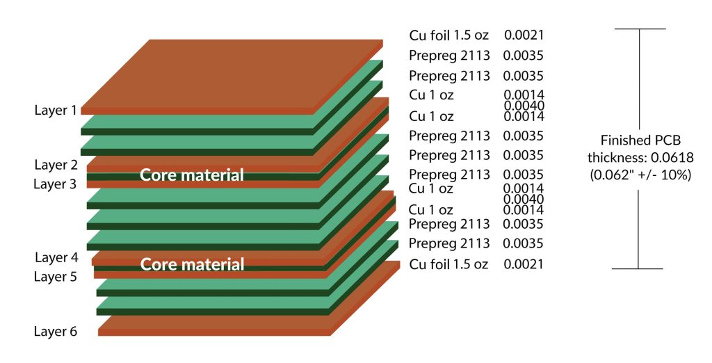
Rigid PCB design relies on fundamental principles of materials, electrical theory, and geometry to ensure functionality. The substrate, typically FR-4, provides mechanical rigidity with a dielectric constant around 4.5, influencing signal propagation speeds. Copper thickness, often 1 oz per square foot, determines current-carrying capacity based on trace width and length. Vias connect layers, with their size affecting drill feasibility and inductance. Hobbyists must balance board size, component density, and layer count to meet project needs. Adhering to these principles forms the rigid PCB design basics.
Layer stackup defines isolation and crosstalk control in multi-layer boards. Signal layers alternate with ground or power planes to minimize noise. Impedance matching becomes relevant for high-speed signals, though hobbyist designs often prioritize DC paths. Thermal vias dissipate heat from power components, preventing hotspots. Beginners should visualize the 3D structure early to avoid routing conflicts.
Design rules govern clearances, widths, and spacings to prevent shorts and ensure etchability. Minimum trace width depends on fabrication limits, typically starting at 0.15 mm for hobbyist boards. Annular rings around pads provide robust soldering joints. IPC-2221B outlines generic design guidelines for trace widths based on current and temperature rise, helping hobbyists calculate safe dimensions. Plane splits require stitching vias to maintain continuity. These mechanisms ensure boards perform reliably in real-world conditions.
Rigid PCB Design Steps: A Beginner Tutorial
Follow these rigid PCB design steps for a structured workflow from concept to Gerber files. Start by defining requirements: list components, power needs, size constraints, and environmental factors like temperature range. Create a schematic capturing connections logically, verifying netlist integrity with connectivity checks. This phase solidifies the electrical design before physical layout.
Next, import the netlist into design software and place components intuitively. Position high-speed parts near connectors, decoupling capacitors close to ICs, and group analog/digital sections separately. Board outline sets the perimeter, incorporating mounting holes for stability. Free rigid PCB design software options exist for hobbyists, offering intuitive interfaces without steep learning curves.
Routing traces follows placement: autoroute where possible, then manually refine critical nets. Prioritize wide traces for power, shorter paths for signals, and avoid right angles to reduce reflections. Use vias sparingly, fanning out from BGA-like packages if needed. Differential pairs require equal lengths for balanced signals.
Run design rule checks (DRC) to flag violations like insufficient clearances or unconnected nets. Review layer utilization and add test points for debugging. Generate fabrication files including drill charts and panelization if scaling up. Iterate based on feedback, simulating basic performance if tools allow. These rigid PCB design steps yield manufacturable boards ready for assembly.
IPC-6012E specifies qualification for rigid boards, guiding hobbyists on performance criteria like conductor spacing and plating thickness during review.
Best Practices for Simple Rigid PCB Design
Optimize rigid PCB design basics with these actionable practices suited for electronic hobbyists. Maintain consistent ground planes to lower impedance and EMI, stitching edges with vias every few millimeters. Decouple power rails at every IC with 0.1 uF ceramics near pins. Thermal reliefs on pads ease soldering for through-hole parts.
For simple rigid PCB design, limit to 2-4 layers unless complexity demands more, reducing cost and warpage risks. Control impedance roughly by layer spacing and trace width for hobby frequencies under 100 MHz. Fiducials aid pick-and-place alignment in future assemblies.
Follow J-STD-020E for handling moisture sensitivity, baking boards if stored long-term before assembly. Document silkscreen clearly with polarity marks and values. Panelize multiples for efficiency, adding breakaway tabs. These habits elevate prototypes to production quality.
Common Mistakes and Troubleshooting in Rigid PCB Design
Beginners often overlook power distribution, leading to voltage drops; calculate trace resistance early using IPC-2221B formulas. Overcrowded placements cause routing jams, so iterate placements liberally. Ignoring fab limits like aspect ratios results in open vias; aim for 8:1 drill-to-board thickness max.
Warpage from asymmetric stackups twists boards; balance copper pour areas. Signal loops pick up noise, so shield with guards or planes. Troubleshoot by probing nets post-assembly, reflowing suspect joints. Visual inspections catch bridges before power-up. Learning from these fixes refines rigid PCB design for dummies approaches.
Conclusion
Mastering rigid PCB design empowers electronic hobbyists to prototype reliably and scale projects confidently. From grasping rigid PCB design basics to executing detailed rigid PCB design steps, this tutorial equips beginners with logical tools for success. Embrace best practices like DRC and stackup planning to avoid pitfalls. Free rigid PCB design software makes entry accessible, fostering creativity in simple rigid PCB design. Apply these insights to your next build, iterating toward perfection. Your journey into custom electronics starts here.
FAQs
Q1: What are the rigid PCB design basics every hobbyist should know?
A1: Rigid PCB design basics include understanding layers, traces, vias, and clearances for reliable circuits. Start with single or double-sided boards using FR-4 substrate for stability. Define schematics first, place components logically, and route with design rules to prevent shorts. Follow IPC guidelines for widths and spacings. These fundamentals ensure simple rigid PCB design works without fabrication issues. Practice on small projects to build intuition.
Q2: Can you outline the key rigid PCB design steps for beginners?
A2: Key rigid PCB design steps are: define requirements, create schematics, place components, route traces, run DRC, and generate files. Import netlists into free software for layout. Prioritize power paths and minimize vias. Review for thermal and signal issues. Export Gerbers for fab. This rigid PCB design tutorial streamlines hobbyist workflows, reducing errors from schematic to board.
Q3: What free tools help with rigid PCB design software free options?
A3: Rigid PCB design software free options provide schematic capture, layout, and DRC for hobbyists. Look for open-source or community editions with intuitive GUIs supporting up to 4 layers. They handle netlists, autorouting, and 3D previews without watermarks. Export standard formats for any fab house. Start with tutorials for simple rigid PCB design to master basics quickly. These tools democratize professional results.
Q4: How to avoid mistakes in rigid Pane PCB design for dummies?
A4: In rigid PCB design for dummies, avoid overcrowding by spacing components 0.5 mm minimum. Calculate power traces to limit voltage drop under load. Balance layers to prevent warpage. Use ground planes and decoupling everywhere. Run simulations if available, and prototype iteratively. Common fixes include wider traces and fiducials. These tips yield robust boards for reliable hobby projects.
References
IPC-2221B — Generic Standard on Printed Board Design. IPC, 2012
IPC-6012E — Qualification and Performance Specification for Rigid Printed Boards. IPC, 2017
J-STD-020E — Moisture/Reflow Sensitivity Classification of Nonhermetic Surface Mount Devices. JEDEC, 2014


