Introduction
In the world of electronic hobby projects, PCB routing plays a pivotal role in turning a schematic into a functional board. Efficient PCB routing strategies ensure that signals travel cleanly between components, minimizing interference and maximizing board performance. For hobbyists designing custom circuits for drones, sensors, or audio amplifiers, poor routing can lead to noise issues, overheating, or outright failures. PCB routing in PCB design involves creating pathways, or traces, that connect components while adhering to electrical and physical constraints. This process demands a balance between space efficiency, signal integrity, and manufacturability. By mastering effective methods for routing in PCB, hobbyists can produce reliable boards on the first try, saving time and resources.
Understanding the basics of PCB routing methods empowers makers to experiment confidently with complex layouts. Whether you're routing a simple Arduino shield or a multi-layer sensor array, thoughtful routing reduces debugging hours. Industry guidelines, such as those in IPC-2221, emphasize systematic approaches to trace placement and layer usage. This article explores proven strategies tailored for electronic hobbyists, from planning to execution. You'll learn how to optimize your designs for better efficiency without advanced equipment.
What Is PCB Routing and Why It Matters in PCB Design
PCB routing refers to the process of defining conductive paths on a printed circuit board to interconnect components as per the schematic. These paths, known as traces, carry signals, power, and ground between pins. In PCB design routing, hobbyists must consider factors like trace width for current capacity, spacing to prevent shorts, and length to avoid timing issues. Routing can be manual, where the designer draws each trace, or assisted by software algorithms, but human oversight ensures optimal results.
The importance of efficient PCB routing strategies cannot be overstated for hobby projects. Poor routing leads to electromagnetic interference (EMI), crosstalk between adjacent traces, or excessive voltage drops in power lines. For instance, in a high-speed data line for a hobby oscilloscope interface, uneven trace lengths can skew signals. Effective methods for routing in PCB also impact manufacturability; tight bends or insufficient clearances complicate fabrication. According to IPC standards like IPC-6012, boards must meet performance specs for reliability in real-world use. Hobbyists benefit from routing that supports easy prototyping and iteration.
Moreover, good routing enhances board compactness, crucial for wearable gadgets or compact enclosures. It allows more components in limited space without sacrificing functionality. As projects scale from single-layer to multi-layer boards, routing decisions influence thermal management and mechanical stability. Prioritizing routing early in the design flow streamlines the entire PCB development process.
Key Technical Principles Behind PCB Routing Methods
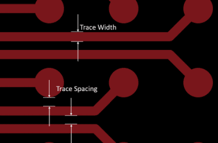
At its core, PCB routing methods rely on electrical engineering principles to maintain signal integrity and power delivery. Trace width determines current-carrying capacity and resistance; wider traces handle higher currents with less heat buildup. Spacing between traces prevents arcing and crosstalk, especially in high-frequency signals. Differential pairs, used for USB or Ethernet in hobby projects, require matched lengths and controlled impedance for balanced transmission.
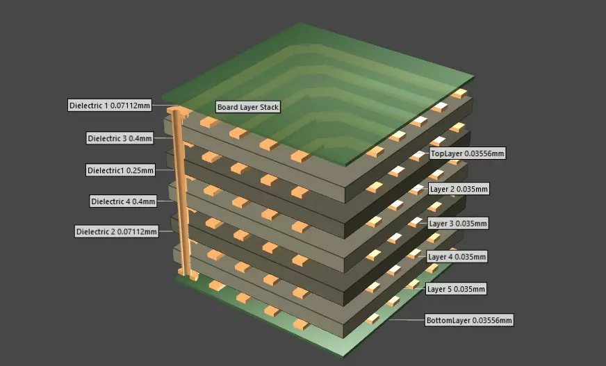
Layer stackup is foundational in PCB design routing. Signal layers alternate with power and ground planes to shield traces and provide low-impedance returns. Vias, vertical interconnects, transition signals between layers but introduce inductance if overused. Hobbyists should calculate via sizes based on drill diameters feasible for standard fabrication. Length matching ensures signals arrive simultaneously, critical for clocks or data buses in synchronous circuits.
Impedance control is another principle, particularly for high-speed hobby designs like RF modules. Uncontrolled impedance causes reflections and signal distortion. Ground planes reduce loop inductance, minimizing EMI emissions. Adhering to guidelines from J-STD standards helps predict board behavior before fabrication.
Bend radii also matter; sharp 90-degree corners create reflections in fast signals, so 45-degree angles or curves are preferable. These principles form the backbone of efficient PCB routing strategies.
Practical Solutions: Best Practices for Efficient PCB Routing Strategies
Start with a solid plan before diving into traces. Review the schematic for critical nets like clocks, high-speed data, and power rails, routing them first to secure optimal paths. Use a grid system for alignment, ensuring traces snap to consistent intervals for symmetry and ease of adjustment. In PCB routing in PCB design, prioritize shortest paths for signals to reduce latency and capacitance.
Incorporate power and ground planes generously. Solid planes provide uniform distribution and act as shields, reducing noise pickup in analog hobby circuits like audio preamps. Fence off sensitive areas with guard traces tied to ground. For multi-layer boards, dedicate inner layers to power and ground, routing signals on outer layers for easy access during assembly.
Minimize vias by planning component placement thoughtfully. Group components by function to shorten interconnects; for example, place decoupling capacitors near IC power pins. Use blind or buried vias in complex designs to save surface space, though they raise costs, so hobbyists often stick to through-hole vias. Fanout pins properly, especially for BGA packages in advanced projects, ensuring escape routes don't cross.
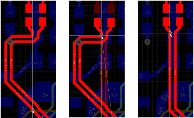
Route differential pairs as pairs, maintaining constant spacing and avoiding splits. Length-tune traces using serpentine patterns for matching without excess length. Avoid routing under crystals or inductors to prevent coupling. These effective methods for routing in PCB streamline fabrication and boost reliability.
Employ hierarchical routing: route power first, then fast signals, followed by slow ones. This order prevents rework. Check for acute angles less than 45 degrees and smooth them. Simulate if possible, but visual DRC (design rule checks) catches most issues.
For hobbyists, single-layer routing suits simple projects: keep traces wide, use jumpers sparingly. Transition to two-layer for more complexity, with ground on the bottom. Multi-layer unlocks efficiency for dense boards.
Common Pitfalls in PCB Design Routing and How to Avoid Them
One frequent mistake is neglecting thermal reliefs on power vias, causing solder issues during hand assembly. Always add spokes or thermal pads for heat dissipation. Overcrowding traces leads to violations; step back and replan placement.
Ignoring return paths creates ground loops, amplifying noise in audio or sensor projects. Ensure every signal trace has a nearby ground return. Excessive vias in high-speed lines add stubs that reflect signals; consolidate where possible.
Unequal trace lengths in buses cause skew; use meanders to equalize. Routing power over signal planes induces coupling; separate them vertically.
Regular DRC runs and 3D previews reveal clearances and overlaps early.
Conclusion
Mastering efficient PCB routing strategies transforms hobby PCB projects from trial-and-error to precise engineering. By understanding principles like impedance control, layer planning, and critical net prioritization, designers achieve compact, reliable boards. Practical steps such as routing high-speed signals first, using planes effectively, and minimizing vias directly enhance performance. These methods align with industry standards, ensuring manufacturability. Hobbyists gain confidence tackling ambitious designs, from IoT devices to robotics. Apply these insights iteratively to refine your workflow and maximize efficiency.
FAQs
Q1: What are the most effective methods for routing in PCB for beginners?
A1: Efficient PCB routing strategies start with planning: identify critical signals and route them first on dedicated layers. Use wide traces for power, maintain clearances per design rules, and employ ground planes for shielding. Avoid sharp bends and minimize vias. This approach, guided by IPC-2221 principles, ensures signal integrity in hobby projects like sensor boards. Practice with simple two-layer designs to build skills.
Q2: How do PCB routing methods impact signal integrity in hobby designs?
A2: PCB routing in PCB design affects integrity through trace length matching, impedance control, and spacing. Matched lengths prevent timing skew in data lines, while proper widths reduce resistance. Ground planes lower EMI. Poor methods cause crosstalk or reflections, degrading performance in high-speed hobby circuits. Follow structured prioritization for clean signals.
Q3: What role do layers play in PCB design routing efficiency?
A3: Layers enable separation of signals, power, and ground, boosting efficiency in dense boards. Outer layers suit easy access, inner for shielding. Effective methods for routing in PCB assign planes strategically, reducing noise. Hobbyists benefit from two- to four-layer stackups for complex projects without excessive cost. Plan stackup early for optimal flow.
Q4: Can autorouting replace manual techniques in PCB routing methods?
A4: Autorouting speeds up PCB routing methods but often needs manual tweaks for optimal paths. It excels for non-critical nets but struggles with dense or high-speed routing. Combine both: auto for bulk, manual for priorities. This hybrid ensures efficient PCB routing strategies tailored to hobby constraints.
References
IPC-2221B — Generic Standard on Printed Board Design. IPC, 2003
IPC-6012DS — Qualification and Performance Specification for Double-Sided Rigid Printed Boards. IPC, 2015
J-STD-001G — Requirements for Soldered Electrical and Electronic Assemblies. IPC/JEDEC, 2011


