Introduction
Multilayer PCB design opens up a world of possibilities for electronic hobbyists looking to build compact, high-performance circuits. Unlike single or double-layer boards, multilayer PCBs stack multiple layers of conductive material separated by insulating layers, allowing for denser layouts and improved functionality. This guide is crafted for beginners eager to master the art of designing a multilayer board. Whether you are working on a personal project or exploring advanced electronics, this multilayer PCB design tutorial will walk you through each step. From understanding the basics to using PCB design software for beginners, you will learn how to design multilayer PCB layouts with confidence. Let us dive into the essentials and build a foundation for creating efficient and reliable boards.
What Is Multilayer PCB Design and Why It Matters
A multilayer PCB consists of three or more conductive layers, typically made of copper, separated by insulating materials known as prepreg or core. These boards are essential for modern electronics where space is limited and complexity is high. Think of smartphones, medical devices, or automotive systems, all relying on multilayer designs to pack numerous components into tiny footprints.
The importance of multilayer PCB design lies in its ability to enhance signal integrity, reduce electromagnetic interference, and support high-speed circuits. For hobbyists, this means you can create more sophisticated projects without sacrificing performance. By following an easy PCB design guide, beginners can tackle challenges like crosstalk or power distribution issues. Mastering this skill also prepares you for advanced applications, making it a valuable step in your electronics journey.
Technical Principles of Multilayer PCB Design
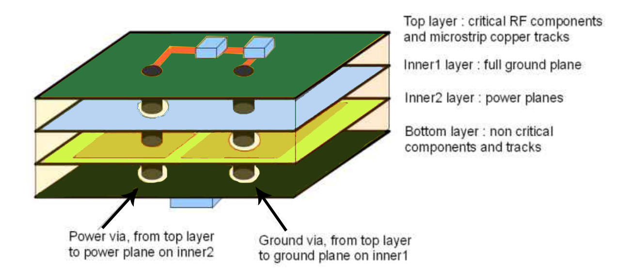
Understanding the core principles of multilayer PCB design is crucial before starting your first project. The structure, or stackup, defines how layers are arranged. A typical four-layer board might include a top signal layer, a ground plane, a power plane, and a bottom signal layer. This setup helps manage signal paths and minimizes interference.
Layer stackup impacts impedance control, which is vital for high-speed signals. Consistent spacing and material properties ensure signals travel without distortion. Another principle is via usage. Vias are small holes connecting layers, and their placement affects signal quality. Blind and buried vias, though complex, save space in dense designs.
Thermal management is also key. Multiple layers can trap heat, so proper copper distribution and thermal vias help dissipate it. For hobbyists, adhering to these principles ensures your board performs reliably under various conditions. Standards like IPC-6012E provide guidelines for layer construction and performance, ensuring your design meets industry expectations.
Step-by-Step Guide to Designing a Multilayer PCB
This section offers a practical, easy PCB design guide tailored for beginners. Follow these steps to create your first multilayer board using PCB design software for beginners.
Step 1: Define Your Project Requirements
Start by outlining your circuit needs. Determine the number of components, power requirements, and signal types. For hobbyists, a four-layer board often suffices for moderate complexity. This initial planning helps decide the layer count and stackup.
Step 2: Choose the Right Design Software
Select a user-friendly PCB design software for beginners. Many tools offer free versions with multilayer support. Look for features like schematic capture, layout editing, and design rule checks. These functions simplify the design process and catch errors early.
Step 3: Create a Schematic
Draw your circuit schematic first. Place components logically, grouping related parts together. Ensure all connections are clear before moving to the layout. A well-organized schematic reduces errors in the multilayer PCB design tutorial process.
Step 4: Plan Your Layer Stackup
Decide on the arrangement of signal, ground, and power layers. A common four-layer setup dedicates inner layers to ground and power for noise reduction. Follow guidelines from standards like IPC-A-600K to ensure proper layer separation and material selection.

Step 5: Place Components on the Board
Position components on the top and bottom layers, keeping high-speed signals away from noisy areas. Group related components to shorten trace lengths. This step is critical for maintaining signal integrity in a multilayer design.
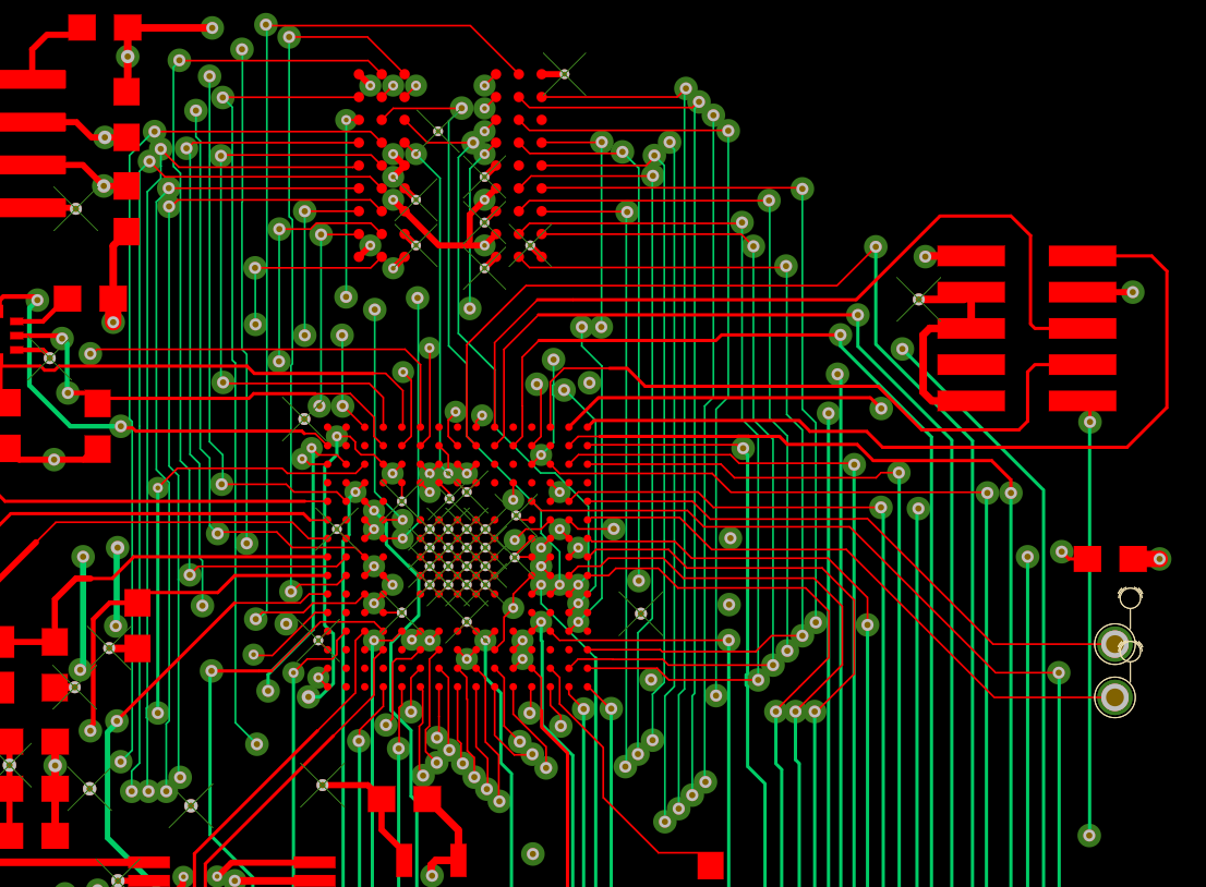
Step 6: Route Traces and Assign Vias
Route critical signals first, using inner layers for power and ground planes. Place vias strategically to connect layers without overcrowding. Avoid crossing high-speed traces over split planes to prevent signal issues.
Step 7: Perform Design Rule Checks
Use your software to check for spacing, clearance, and connectivity errors. Standards like IPC-6012E outline acceptable tolerances for trace widths and via sizes. Correct any violations to ensure manufacturability.
Step 8: Generate Output Files
Once your design is error-free, export the necessary files for manufacturing. These typically include Gerber files for each layer and a drill file for vias. Double-check the output to avoid costly mistakes during production.
Best Practices for Multilayer PCB Design
Adopting best practices elevates your design quality and reliability. These tips are tailored for hobbyists learning how to design multilayer PCB layouts.
- Keep ground planes continuous on inner layers to reduce noise.
- Use adequate via sizes based on current requirements to prevent overheating.
- Maintain consistent trace impedance for high-speed signals by controlling layer spacing.
- Avoid placing components or traces near board edges to prevent damage.
- Test your design with simulation tools if available in your software.
Following these practices, aligned with standards like IPC-A-600K, ensures your board meets performance expectations. Regular reviews during design also catch potential issues early.
Common Challenges and How to Overcome Them
Beginners often face hurdles in multilayer PCB design. One issue is signal crosstalk, where adjacent traces interfere. Solve this by increasing spacing or using ground planes as shields. Another challenge is thermal buildup in dense designs. Address this by adding thermal vias to transfer heat to outer layers.
Manufacturing errors, like misalignment of layers, can occur if files are incorrect. Always verify output files against design rules. For hobbyists, starting with simpler four-layer designs builds confidence before tackling complex boards. Refer to standards like IPC-6012E for acceptable limits on layer registration and tolerances.
Conclusion
Designing a multilayer PCB as a beginner may seem daunting, but with the right approach, it becomes an achievable skill. This multilayer PCB design tutorial has covered the essentials, from understanding layer stackups to routing traces effectively. By following the step-by-step guide and best practices, hobbyists can create reliable boards for their projects. Remember to leverage PCB design software for beginners and adhere to recognized standards for quality. With practice, you will gain confidence in how to design multilayer PCB layouts, opening doors to more complex electronic creations.
FAQs
Q1: What is the easiest way to start with multilayer PCB design for beginners?
A1: Starting with multilayer PCB design is simpler with a clear plan. Choose user-friendly PCB design software for beginners and focus on a basic four-layer board. Draw your schematic, plan the stackup with ground and power planes, and route traces carefully. Use design rule checks to avoid errors. Following standards like IPC-6012E helps ensure your first design is manufacturable and functional.
Q2: How do I choose PCB design software for beginners?
A2: Look for software with intuitive interfaces and free or low-cost versions supporting multilayer designs. Features like schematic capture, layout tools, and error checking are essential. Ensure it offers tutorials or community support for learning. Many tools align with industry standards like IPC-A-600K, helping you create accurate designs without needing advanced skills early on.
Q3: What are common mistakes in a multilayer PCB design tutorial process?
A3: Beginners often overlook layer stackup planning, leading to signal issues. Poor via placement can cause connectivity problems, and ignoring thermal management risks overheating. Not running design rule checks may miss spacing errors. Stick to guidelines from standards like IPC-6012E to avoid these pitfalls and review your design at each step for better results.
Q4: Why is layer stackup important in how to design multilayer PCB?
A4: Layer stackup defines how signal, ground, and power layers are arranged, impacting noise and signal quality. A proper stackup reduces interference and ensures stable power distribution. For hobbyists, a balanced stackup like signal-ground-power-signal in a four-layer board is ideal. Standards like IPC-A-600K provide rules for layer spacing and materials to achieve reliable performance.
References
IPC-6012E — Qualification and Performance Specification for Rigid Printed Boards. IPC, 2020.
IPC-A-600K — Acceptability of Printed Boards. IPC, 2020.


