Introduction
In modern electronics, RF applications demand printed circuit boards that handle signals from hundreds of megahertz to tens of gigahertz with minimal degradation. Multilayer PCBs play a critical role in these systems by providing the density and isolation needed for complex RF circuits found in telecommunications, radar, and wireless infrastructure. At high frequencies, conventional design approaches fail due to increased signal losses and interference, making specialized RF PCB design essential. This article explores key strategies for multilayer PCB design tailored to RF, focusing on high-frequency PCB layout, materials, impedance matching, and signal integrity. Engineers must prioritize these elements to achieve reliable performance in demanding environments. By understanding these principles, designers can optimize multilayer stacks for superior RF operation.
Understanding Multilayer PCBs in RF Applications
Multilayer PCBs consist of multiple conductive layers separated by insulating dielectrics, interconnected via plated through-holes or advanced via structures. In RF contexts, these boards support transmission lines that propagate signals as electromagnetic waves, unlike low-frequency designs where lumped elements dominate. The shift to distributed effects at high frequencies necessitates careful control over geometry and materials to prevent reflections and attenuation. RF PCB design thus revolves around maintaining characteristic impedance and minimizing discontinuities. Why does this matter for electric engineers? Poor design leads to reduced range, higher bit error rates, and compliance failures in systems like 5G base stations or satellite communications.
The relevance intensifies with the proliferation of high-frequency applications pushing beyond 10 GHz. Multilayer configurations allow dedicated signal layers flanked by ground planes, reducing crosstalk and radiation. However, fabrication tolerances become critical, as even minor variations in dielectric thickness alter electrical properties. Standards like IPC-2221C guide generic design requirements, ensuring boards meet performance criteria across layers.
Core Technical Principles in High-Frequency RF PCB Design
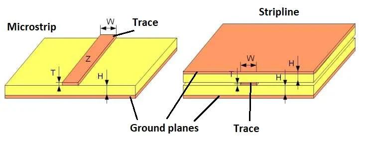
At high frequencies, signals behave as transmission lines governed by Maxwell's equations, where wavelength approaches board dimensions. Key challenges include skin effect, which confines current to conductor surfaces, increasing effective resistance, and dielectric losses proportional to the dissipation factor (Df). RF PCB materials must exhibit low dielectric constant (Dk) to support faster propagation and low Df to curb attenuation. Conductor roughness exacerbates losses, so smooth copper foils are preferred in multilayer builds. Transmission line types, such as microstrip on outer layers or stripline embedded between grounds, dictate field confinement and shielding effectiveness.
Impedance in RF PCB design is fundamentally Z0 = sqrt(L/C), where inductance (L) and capacitance (C) depend on trace width, thickness, and dielectric properties. Mismatches cause reflections quantified by return loss, degrading signal integrity. In multilayer stacks, asymmetry leads to modal dispersion, splitting signals into even and odd modes with different velocities. Ground planes provide return paths, but via fences or stitching mitigate slotline modes that radiate energy. These principles underpin high-frequency PCB layout, demanding precise modeling of fields.
Dielectric behavior varies with frequency, as Dk decreases and Df rises in some materials, impacting phase stability. Thermal expansion mismatches between layers cause warpage, altering impedances post-fabrication. IPC-6018D specifies qualification for high-frequency boards, emphasizing electrical testing like time-domain reflectometry for discontinuities.
Selecting RF PCB Materials for Optimal Performance
Material choice dominates RF PCB design due to their direct influence on loss tangent and stability. Low-loss dielectrics minimize insertion loss, expressed as alpha = (pi f / c) * sqrt(epsilon_r) * tan delta, where frequency (f) amplifies Df effects. Multilayer RF PCBs often hybridize cores with different properties: low Dk/Df for signal layers and cost-effective fillers for non-critical areas. Coefficient of thermal expansion (CTE) matching prevents delamination under thermal cycling common in RF power amps. Copper type matters too, with electrodeposited foils offering smoothness for reduced skin effect losses.
Fabrication compatibility guides selection, as high-frequency materials may require special lamination pressures to avoid voids. Prepregs fill gaps in multilayer presses, influencing final Dk uniformity. Engineers evaluate materials via split-post resonators or stripline tests for accurate Df at operating frequencies. Stability over humidity and temperature ensures long-term RF PCB signal integrity.
High-Frequency PCB Layout Best Practices
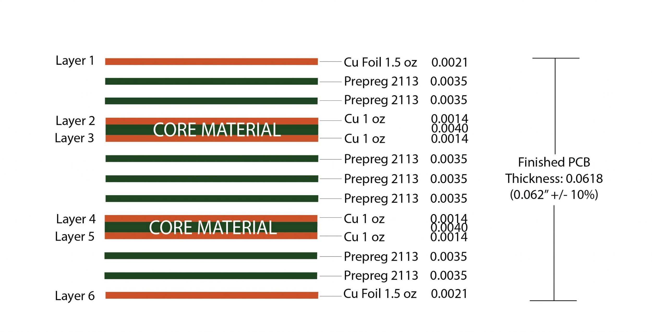
Effective high-frequency PCB layout begins with stackup planning, aiming for symmetry to balance mechanical stress and electrical fields. Place high-speed RF signals between ground planes for stripline configuration, confining fields and suppressing radiation. Route traces as straight as possible, avoiding right-angle bends that introduce reflections; use 45-degree mitered corners instead. Maintain minimum spacing per the 3W rule, where trace separation exceeds three times width to cut crosstalk below -30 dB. Ground vias surround signal vias to preserve impedance during transitions.
RF PCB impedance matching employs distributed elements like open or shorted stubs for filters and baluns. Decoupling capacitors near IC pins shunt noise to ground, with via placement minimizing inductance. Power integrity ties into RF, as plane resonances couple to signals; segmented planes with stitching vias help. Simulate S-parameters to verify return loss better than 10 dB across bandwidth.
Via design poses challenges in multilayer RF PCBs, as through-hole stubs reflect at quarter-wave frequencies. Blind, buried, or back-drilled vias reduce stub length, preserving signal integrity. Controlled depth drilling aligns with IPC guidelines for hole quality.
Ensuring RF PCB Signal Integrity and Impedance Control
Signal integrity in RF PCB design hinges on minimizing discontinuities that cause ringing or attenuation. Characteristic impedance control requires consistent trace geometry, with width calculators accounting for etch tolerances. T-match or pi-networks at interfaces match disparate impedances, calculated via Smith charts. Crosstalk arises from mutual inductance and capacitance; coplanar waveguide (CPW) with ground on both sides enhances isolation.
Radiation from traces occurs if return currents spread, so solid ground pours under signals are vital. Guard traces or shielding walls further contain emissions. Testing involves vector network analyzers for S21 insertion loss and eye diagrams for digital-RF hybrids. Troubleshooting mismatches often reveals unaccounted fringing fields at bends.
Common pitfalls include neglecting via capacitance in dense multilayer stacks, inflating effective length. Thermal vias under hot spots prevent hotspots distorting dielectrics.
Practical Troubleshooting in Multilayer RF PCBs
Engineers encounter issues like unexpected resonances from cavity effects between planes. Adjust stackup spacing or add lossy materials to dampen. Excessive loss points to rough copper or high Df; polish or select reverse-treated foil. Fabrication variances, such as dielectric thickness drift, shift impedances; specify tight tolerances per IPC-6018D.
Phase imbalance in differential pairs stems from unequal lengths; length-match within wavelength/20. Simulate full 3D EM fields for accuracy beyond 2D approximations.
Conclusion
Multilayer PCB design for RF applications demands a holistic approach integrating RF PCB materials, high-frequency PCB layout, impedance matching, and signal integrity measures. By prioritizing low-loss dielectrics, symmetric stackups, and discontinuity-free routing, engineers optimize performance at high frequencies. Adhering to standards like IPC-2221C and IPC-6018D ensures manufacturability and reliability. These practices enable robust RF systems with minimal losses and maximal bandwidth. Future designs will leverage even higher frequencies, underscoring the need for ongoing refinement in RF PCB design techniques.
FAQs
Q1: What materials are best for RF PCB design at frequencies above 10 GHz?
A2: Low dielectric constant (Dk) and low dissipation factor (Df) materials form the backbone of RF PCB design for high frequencies. These reduce signal attenuation and support controlled propagation. Hybrid stackups combine them with stable cores for multilayer integrity. Selection considers CTE matching to avoid warpage. Always verify properties at target frequencies for optimal RF PCB signal integrity.
Q2: How does high-frequency PCB layout impact impedance matching?
A2: High-frequency PCB layout directly influences RF PCB impedance matching through trace geometry and ground proximity. Symmetric routing and adjacent planes maintain 50-ohm lines. Vias and bends introduce mismatches if unmanaged. Ground stitching preserves return paths. Simulations confirm matching before fabrication.
Q3: Why is signal integrity critical in multilayer RF PCBs?
A3: RF PCB signal integrity prevents losses from crosstalk, reflections, and radiation in multilayer designs. At high frequencies, discontinuities amplify degradation. Ground planes and via optimization isolate signals. Testing verifies low insertion and return loss. This ensures reliable performance in RF applications.
Q4: What role do standards play in RF PCB design?
A4: Standards like IPC-6018D provide qualification criteria for high-frequency boards, covering electrical and mechanical performance. They guide tolerances in multilayer fabrication. Compliance minimizes risks in RF PCB impedance matching and layout. Engineers reference them for consistent, reliable designs.
References
IPC-2221C — Generic Standard on Printed Board Design. IPC, 2023
IPC-6018D — Qualification and Performance Specification for High Frequency (Microwave) Printed Boards. IPC, 2022
IPC-2252 — Design Guide for RF/Microwave Circuit Boards. IPC, 2002


