Introduction
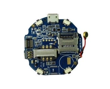
Electronic hobbyists often push the boundaries of creativity by building compact devices such as wearable sensors, miniature drones, and portable IoT modules. These projects demand PCB design for small electronics that balances functionality, size, and reliability. Optimizing PCB design for small electronics becomes essential to avoid common issues like signal interference, overheating, and manufacturing failures. Small PCBs, typically under 50 square centimeters, require meticulous planning to fit components densely while maintaining electrical performance. This article explores practical strategies to streamline your workflow, drawing on engineering principles tailored for hobbyist-level projects. By focusing on key optimization techniques, you can achieve professional results without advanced tools.
Why PCB Design for Small Electronics Matters
Space limitations in small electronics force designers to maximize every millimeter of board real estate. Poor optimization leads to routing congestion, which compromises signal integrity and increases electromagnetic interference risks. Hobbyists frequently encounter challenges like component overlap or inadequate power distribution in tiny layouts. Effective PCB small electronics design enhances device portability and battery life, critical for applications like fitness trackers or smart badges. Moreover, optimized boards reduce assembly errors and improve yield during prototyping. Understanding these factors ensures your projects transition smoothly from breadboard to production-ready prototypes.
In the hobbyist community, small PCBs enable innovative designs that larger boards cannot accommodate. Thermal management becomes a priority, as dense packing traps heat from active components. Reliability suffers without proper ground planes or decoupling capacitors, leading to erratic behavior in real-world use. Optimizing PCB design small electronics also cuts material costs and speeds up iteration cycles. Hobbyists benefit from designs that align with basic manufacturability rules, avoiding costly respins.
Key Technical Principles for Small PCB Designs
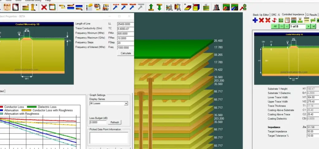
The foundation of PCB design small electronics lies in layer stackup decisions. Single-layer boards suit ultra-simple circuits, but dual or four-layer stacks provide better isolation for signals and power. Ground planes on inner layers shield traces, reducing crosstalk in confined spaces. Trace width calculations follow current-carrying capacity rules to prevent overheating, especially for power rails in battery-powered gadgets. Via placement demands precision, as blind or buried vias save surface area but add complexity. Component footprints must match pad sizes exactly to ensure solder joint strength.
Signal integrity principles guide high-speed trace routing in small designs. Keep traces short and avoid sharp bends, which cause impedance mismatches. Differential pairs for data lines require equal lengths and controlled spacing. Power integrity relies on wide pours and multiple vias to distribute current evenly. Thermal vias under hot components wick heat to inner copper layers. Adhering to IPC-2221B guidelines for generic printed board design helps hobbyists select appropriate clearances and spacings systematically.
Material selection influences performance in PCB small designs. FR-4 laminates offer a cost-effective base with good mechanical stability for hobbyist prototypes. Thinner cores, around 0.8 mm total thickness, enable compact profiles without excessive flex. Copper weight, typically 1 oz per square foot, balances conductivity and etching ease. Dielectric constants affect signal propagation, so consistent materials prevent timing skews. These principles form the backbone of reliable small electronics layouts.
Challenges in Optimizing PCB Design for Small Electronics
High component density in small PCBs amplifies electromagnetic interference issues. Traces running parallel too closely couple noise, degrading analog signals from sensors. Heat dissipation poses another hurdle, as limited copper area concentrates thermal loads from microcontrollers or LEDs. Mechanical stress from warpage during soldering can crack fine-pitch solder joints. Hobbyists often overlook panelization, leading to inefficient fabrication of multiple small boards. Vibration in portable devices exacerbates fatigue in unsupported leads.
Routing congestion arises when trying to fit analog, digital, and power sections together. Without partitioned zones, ground loops induce hum in audio circuits. Vias clutter the board, blocking component placement and increasing inductance. Manufacturing tolerances tighten for small features, like 0.15 mm traces, raising defect risks. Environmental factors, such as humidity, affect insulation resistance in dense layouts. Addressing these systematically elevates PCB design for electronics from trial-and-error to engineered solutions.

Best Practices for PCB Small Electronics Design
Start with a clear schematic to map component interactions before layout. Group related functions into zones: power entry near connectors, sensitive analog away from clocks. Use autorouters sparingly; manual routing ensures optimal paths for critical nets. Maintain at least 0.2 mm clearances between traces and pads for 2-layer boards. Employ teardrops on pads to strengthen connections against drill wander. Decoupling capacitors placed within 5 mm of IC power pins stabilize voltage rails effectively.
Layer assignment optimizes signal flow in multi-layer small designs. Dedicate outer layers to components and signals, inners to power and ground. Stitch ground planes with vias every 10 mm to lower impedance. For RF sections, implement coplanar waveguides with ground on the same layer. Thermal reliefs on pads ease hand-soldering for prototypes. Following J-STD-001 requirements for soldered assemblies ensures joint reliability in hobbyist builds.
Component orientation streamlines assembly and trace lengths. Align IC pins parallel to the board edge for easier access. Select packages like QFN or 0402 for density, verifying thermal pads connect properly. Fiducials aid pick-and-place alignment if scaling to production. Simulate power distribution early to spot voltage drops. Panelize boards with 2-3 mm v-grooves between units for cost-effective fab runs.
Power management techniques shine in battery-constrained small electronics. Use ferrite beads on input lines to filter noise. Star-point grounding converges returns at one spot, minimizing loops. Wide traces, at least 0.5 mm for 1A currents, prevent IR drops. Sleep modes in firmware complement hardware by reducing quiescent draw. These practices make PCB design small electronics efficient and robust.
Troubleshooting Common Issues in Small PCB Designs
Hobbyists often face intermittent failures traced to poor grounding. Floating grounds create noise floors that swamp weak signals from sensors. Solution: Flood unassigned areas with ground pours, connected via stitching vias. Overheating ICs signal inadequate heatsinking; add copper pours and vias under dies. Solder bridges on fine-pitch parts stem from oversized pads; refine footprints and use flux judiciously.
Warpage distorts small boards post-reflow, misaligning components. Thinner laminates exacerbate this; choose balanced stackups per IPC-A-600 acceptability criteria. Test prototypes with a straightedge for flatness. Crosstalk in digital lines manifests as glitches; increase separation or add shielding traces. Iterate with thermal imaging if available, or monitor temperatures via thermocouples. These fixes turn problematic prototypes into reliable hobby projects.
Conclusion
Optimizing PCB design for small electronics empowers hobbyists to create compact, high-performance devices with confidence. Key principles like strategic layering, precise routing, and thermal management address the unique constraints of tiny boards. Best practices, from zoning components to robust grounding, minimize pitfalls and enhance manufacturability. By applying these structured approaches, you reduce prototyping cycles and boost project success rates. Whether building wearables or IoT nodes, thoughtful PCB small designs yield durable results. Embrace these techniques to elevate your electronic hobbyist endeavors.
FAQs
Q1: How does optimizing PCB design small electronics improve signal integrity?
A1: Optimizing PCB design small electronics involves short traces, ground planes, and controlled impedances to minimize crosstalk and reflections. Hobbyists achieve this by routing high-speed signals away from power lines and using differential pairs where needed. Proper via fencing around sensitive areas further shields noise. These steps ensure clean signals in dense layouts, preventing data errors in compact devices. Overall, they enhance reliability for projects like wireless sensors.
Q2: What are essential clearances in PCB design for small electronics?
A2: In PCB design for small electronics, maintain 0.15-0.25 mm trace-to-trace clearances and 0.2 mm pad-to-trace gaps for reliable etching. Adjust based on layer count and voltage levels to avoid shorts. Ground-to-signal spacing prevents coupling. Hobbyists verify these via design rule checks during layout. Consistent application supports high-density packing without fabrication issues.
Q3: Why use multi-layer boards for PCB small electronics design?
A3: Multi-layer boards in PCB small electronics design separate signals, power, and grounds effectively, reducing interference in tight spaces. They enable buried vias for routing efficiency and better thermal paths. Hobbyists opt for 4 layers when 2-layer routing congests. This approach aligns with standards for performance, fitting more functionality into miniature footprints reliably.
Q4: How to manage heat in optimize PCB design small electronics?
A4: To optimize PCB design small electronics for heat, incorporate thermal vias under hot components and pour copper planes for spreading. Position heat sources near edges for airflow. Thinner boards with inner planes conduct better. Hobbyists monitor via junction temperatures during testing. These methods prevent failures in portable gadgets.
References
IPC-2221B — Generic Standard on Printed Board Design. IPC, 2009
J-STD-001G — Requirements for Soldered Electrical and Electronic Assemblies. IPC, 2011
IPC-A-600K — Acceptability of Printed Boards. IPC, 2020


