What is V-Scoring and Why is it Essential in PCB Manufacturing?
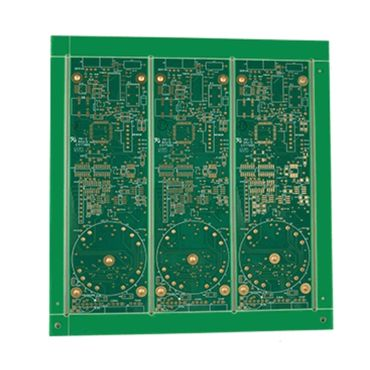
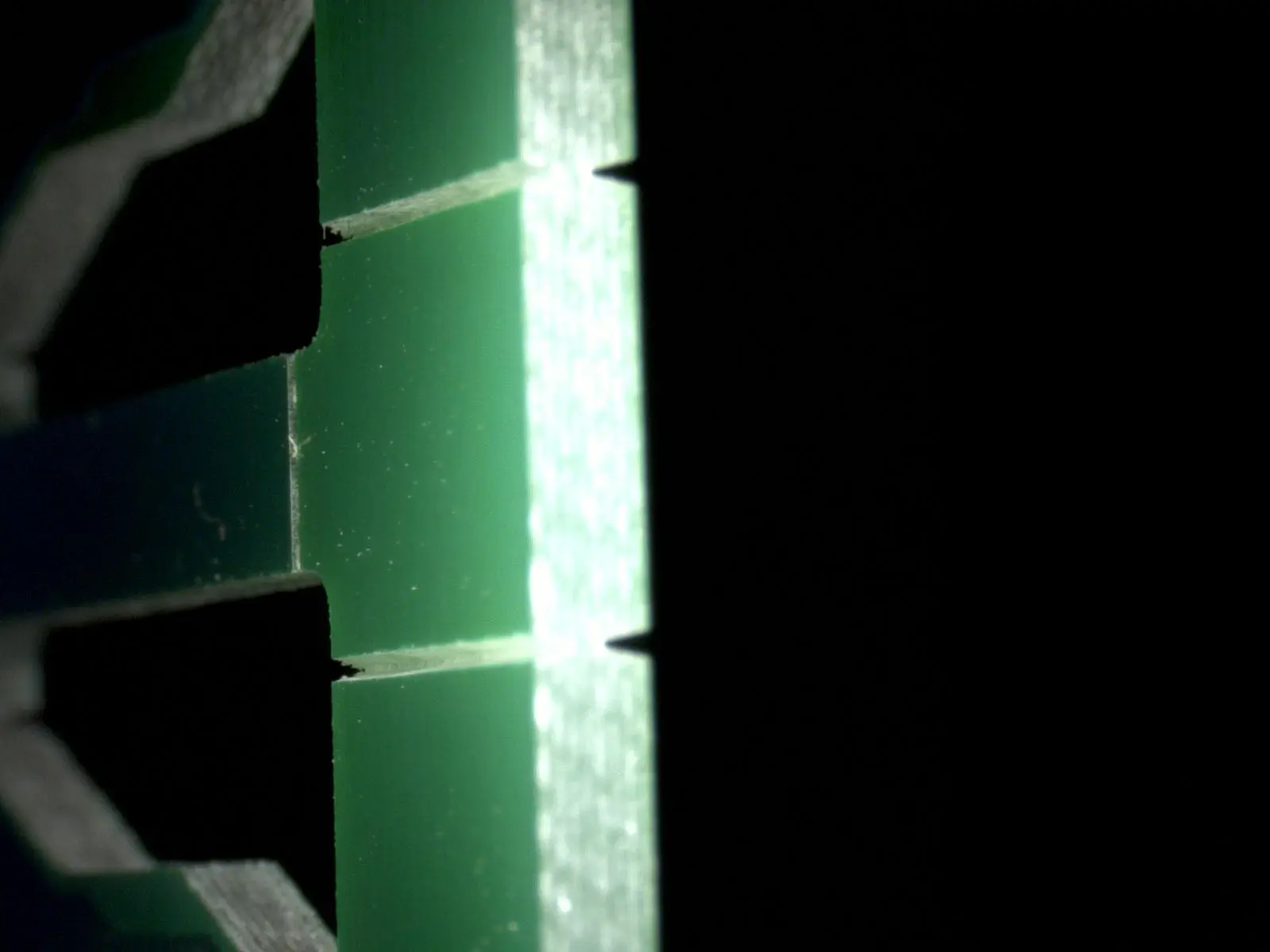
V-scoring, also known as V-grooving or V-cutting, is a widely used technique in printed circuit board (PCB) fabrication. It involves creating precisely cut, V-shaped grooves on both the top and bottom surfaces of a panelized PCB, leaving a thin web of material in the center. This design allows individual boards to be easily separated after the assembly process, much like snapping segments from a chocolate bar.
The primary benefit of V-scoring lies in its ability to significantly enhance manufacturing efficiency. By grouping multiple PCBs onto a single panel, lines of automated surface-mount technology SMT PCB assembly can process more units simultaneously. However, this convenience introduces mechanical stress points within the board. Understanding how these grooves affect structural integrity and, critically, the components placed nearby, is paramount for any PCB designer aiming for a robust and high-performing final product.
How Does V-Scoring Influence Component Layout on a PCB?
The process of placing components on a PCB demands precision, and V-scoring introduces an additional layer of considerations. The grooves inherently weaken the board material along their lines, making these areas vulnerable to stress, potential cracking, or unintentional damage during handling or the final separation step.
Mechanical Stress and Board Integrity
When individual boards are snapped apart from a panel, the mechanical forces can induce vibrations and stress. This stress poses a significant risk to delicate components or their solder joints located in close proximity to the V-score lines. Furthermore, an uneven distribution of stress caused by V-scoring can lead to undesirable board warpage, which might result in component misalignment or compromised electrical connections. Traces routed too near a V-score risk fracturing during separation, potentially causing open circuits or unreliable performance. Consequently, designers must adhere to specific guidelines for component placement to prevent costly reworks and ensure product reliability.
Related Reading: Optimizing PCB Panelization: A Comprehensive Guide to V Scoring for Straight Edged Boards
What Are the Key Design Rules for V-Scoring Component Placement?
To mitigate the risks associated with V-scoring, established design rules focus on optimizing component placement and overall board layout. These guidelines are crucial for ensuring the long-term functionality and durability of your PCB.
Maintaining Component Distance from V-Score Lines
One of the most critical V-scoring design rules is to maintain an adequate clearance between components and the V-score line. As a general guideline, components should be positioned at least 5 mm (0.2 inches) away from the scored edge. For larger or heavier components, such as bulky connectors or electrolytic capacitors, this buffer distance should ideally be increased to 8-10 mm (0.3-0.4 inches) to account for the heightened risk of mechanical shock during board separation. Adhering to this "component distance from V-score" rule is vital in protecting solder joints and component bodies from stress-induced damage, which could otherwise lead to intermittent connections or complete failure.
Defining V-Scoring Keepout Zones
A "V-scoring keepout zone" designates an area on the PCB where no components, traces, or vias are permitted. Typically, this zone extends 3-5 mm (0.12-0.2 inches) on either side of the V-score line, with the exact dimension often dependent on the board's thickness and material. For instance, a standard 1.6 mm thick FR-4 PCB board might require a 3 mm keepout zone, while a thinner 0.8 mm board, being more fragile, would necessitate a wider 5 mm zone. These keepout zones are crucial for preventing damage to components and traces during the scoring and separation processes. They also play a vital role in minimizing the formation of microcracks in the PCB material, which could otherwise propagate over time and compromise the board’s overall reliability.
Advanced Considerations for V-Scoring in PCB Design
Beyond fundamental design rules, several additional factors influence how V-scoring should be integrated into your PCB layout. These considerations help ensure that the board not only functions optimally but also endures the rigors of manufacturing and assembly.
Board Material, Thickness, and Panel Layout
The PCB's thickness and material properties significantly impact how V-scoring affects component placement. Thicker boards (e.g., 2.0 mm or more) are inherently more robust and can generally tolerate components closer to the V-score line, potentially with a minimum distance of around 3 mm. Conversely, thinner boards (e.g., 0.6-0.8 mm) are more susceptible to bending and cracking, thus requiring a wider keepout zone of 5-7 mm. Material choice is also critical; standard FR-4 offers good durability, but more specialized flexible or high-frequency materials like polyimide or Rogers may necessitate larger keepout zones due to their distinct mechanical characteristics. Always consult your manufacturing partner for specific recommendations tailored to your chosen materials. Additionally, the orientation of V-score lines within the panel can influence stress distribution; aligning scores along the shorter edges of a rectangular board might reduce stress compared to scoring along longer edges. It is essential to ensure that the panel layout facilitates a uniform scoring depth, typically 30-50% of the board thickness per side, to prevent uneven stress that could harm nearby components.
Trace Protection and Stress Mitigation
Electrical traces and vias are just as vulnerable to damage as physical components. Routing traces too close to and parallel with a V-score line (within, for example, 3 mm or 0.12 inches) risks fracturing them during board separation, potentially disrupting critical signals. If traces must traverse a V-score area, it is best practice to route them perpendicular to the line, minimizing the length exposed to potential stress. Furthermore, vias should be strictly avoided within the designated keepout zone, as they can further weaken the board structure and act as concentrated points for stress, increasing the likelihood of failure.
Related Reading: Cracking the Code: Optimizing V Scoring for PCB Depaneling Success
Best Practices for Integrating V-Scoring into Your PCB Workflow
To ensure successful PCB designs that effectively balance V-scoring with reliable component placement, several best practices should be adopted throughout your development process. These tips promote both manufacturability and long-term product integrity.
Collaboration, Software Tools, and Documentation
Early and continuous collaboration with your manufacturing partner is paramount. Different fabrication houses possess unique V-scoring capabilities and constraints, so sharing your design files early ensures compliance with their specific processes, particularly concerning groove depth and spacing. Leverage the advanced features available in most PCB design software, which allow you to define custom keepout zones and implement automated rules for component placement relative to V-score lines. This automation helps enforce design guidelines consistently. When planning your layout, prioritize grouping similar components away from V-score lines to streamline assembly and minimize the risk of damage. For example, consolidating all surface-mount technology (SMT) components into a central cluster leaves the board edges clear for safe scoring. Lastly, thoroughly document all V-scoring specifications within your design files, including precise groove depths (e.g., 0.5 mm per side) and minimum component distances, to ensure the manufacturer fully understands and executes your design intent.
Conclusion: Achieving Reliability Through Strategic V-Scoring and Placement
V-scoring stands as an invaluable technique for enhancing the efficiency of PCB manufacturing, yet it introduces critical design challenges directly impacting component placement and overall board reliability. By rigorously adhering to key "V-scoring design rules," maintaining appropriate "component distance from V-score" lines, and meticulously defining "V-scoring keepout zones," designers can significantly mitigate risks and guarantee that their PCBs perform robustly as intended. Whether your project involves a straightforward prototype or a complex multilayer board, thoughtful "V-scoring component placement" is absolutely essential for achieving both manufacturability and sustained reliability.
AIVON, one of the most popular online PCB manufacturer in China, is dedicated to assisting engineers in navigating the complexities of PCB design. By integrating these comprehensive guidelines into your workflow, you will be exceptionally well-equipped to create boards that not only withstand the mechanical stresses inherent to V-scoring but also deliver superior performance. Keep these crucial insights in mind for your upcoming projects, and you will undoubtedly observe a marked improvement in both the quality and efficiency of your PCB designs.


