Introduction
In PCB manufacturing, panelization enables efficient production by grouping multiple boards into a single panel for processing, assembly, and testing. V-scoring stands out as a precise method for straight-edged boards, creating V-shaped grooves that facilitate clean separation without tabs or complex routing. This approach aligns with factory workflows, reducing handling time and material waste while maintaining structural integrity during soldering and reflow. Electrical engineers benefit from V-scoring PCB panel design because it supports high-volume runs with minimal stress on components. Optimizing this technique ensures compliance with production standards and lowers overall costs. As panels move through depanelization, proper V-score implementation prevents defects like cracking or delamination.
What Is V-Scoring?
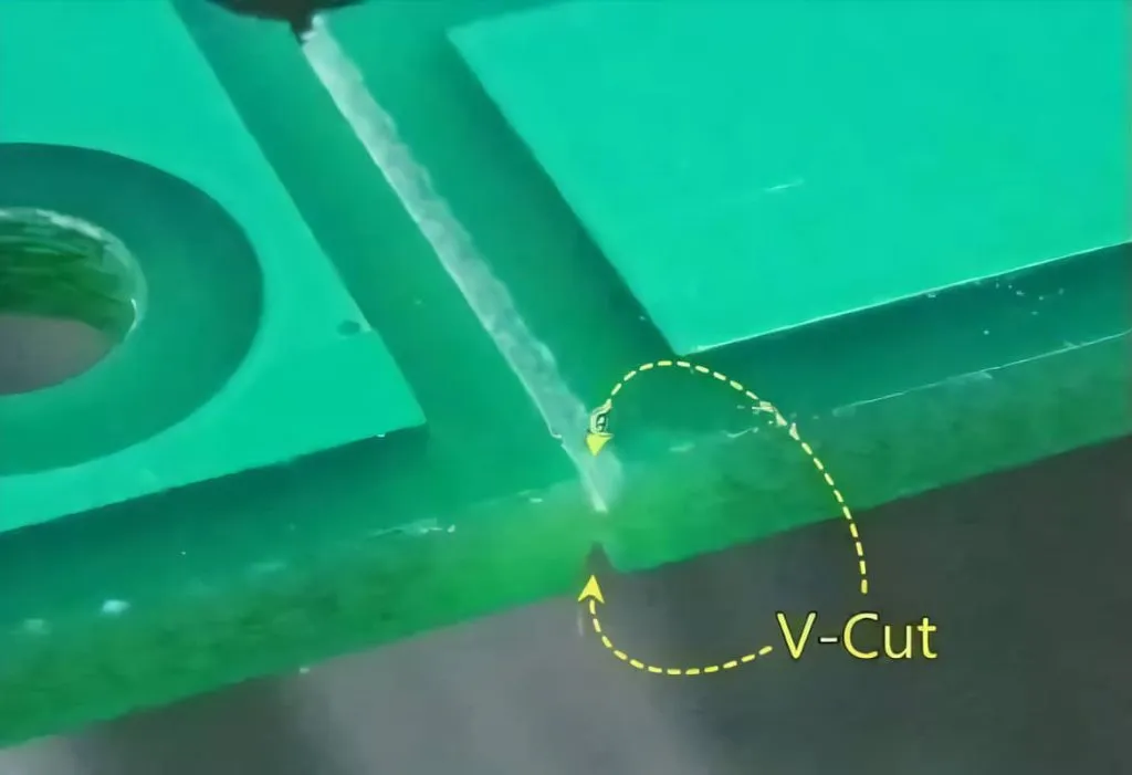
V-scoring involves machining V-shaped grooves into the top and bottom surfaces of a PCB panel along predefined straight lines. These grooves partially remove material, leaving a thin residual web that holds the individual boards together until separation. The process uses specialized routing tools with angled bits to create symmetric cuts, typically at 45-degree or 60-degree angles for optimal break strength. Factory operators perform this during the scoring stage after lamination but before final fabrication steps. Unlike tab routing, V-scoring requires no perforations or breakaway tabs, simplifying the panel structure. This method suits rigid boards with uniform thickness and rectangular outlines.
Why V-Scoring Matters for Straight-Edged Boards
V-scoring enhances throughput in assembly lines by allowing quick manual or automated depanelization without specialized equipment. It maximizes panel utilization, fitting more boards per array and reducing per-unit costs in medium to high-volume production. Straight-edged boards benefit most, as the linear grooves align perfectly with orthogonal layouts common in consumer electronics and industrial controls. Engineers appreciate the reduced risk of burrs or contamination compared to milling methods. Moreover, it preserves panel flatness during reflow, critical for surface-mount technology processes. Overall, V-scoring supports scalable manufacturing while adhering to quality benchmarks.
Technical Principles of V-Scoring
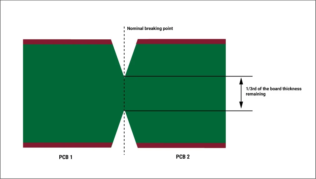
The V-groove forms through simultaneous or sequential passes of a V-bit router, cutting from both sides to meet at the center plane. Groove depth typically reaches two-thirds of the board thickness, leaving one-third intact for stability. Common angles include 45 degrees for finer control or 60 degrees for stronger webs, influencing snap force and edge finish. Material properties like FR-4 glass transition temperature affect groove quality, requiring controlled spindle speeds to avoid resin smear. Post-scoring inspection verifies symmetry and web uniformity using optical comparators. These principles ensure the panel withstands handling stresses up to final assembly.
According to IPC-2221B, the residual thickness in V-scoring should be at least one-third of the total board thickness to maintain mechanical integrity. This guideline prevents premature cracking during transport or thermal cycling.
V-Score Panel Design Rules
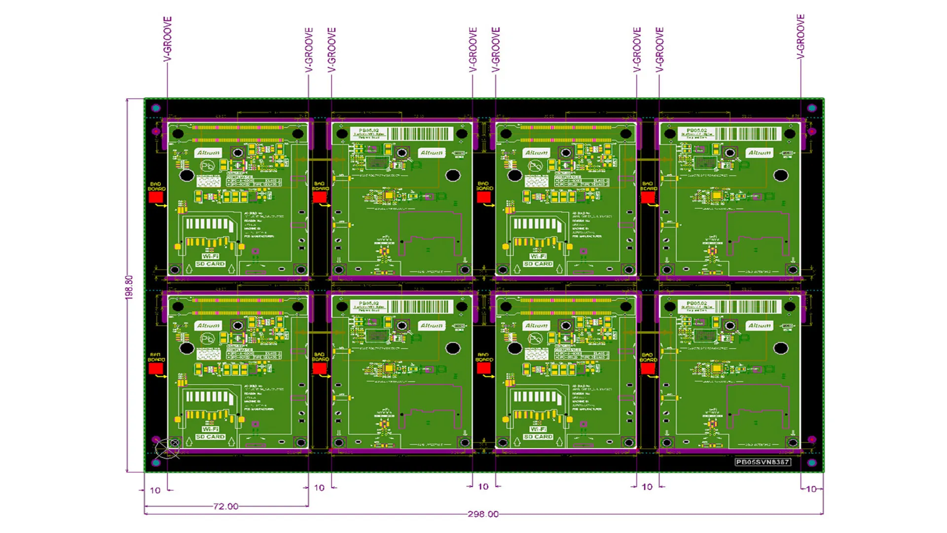
Effective V-scoring PCB panel design starts with aligning boards in a grid pattern with grooves running fully across the panel edges. Minimum board dimensions ensure router stability, typically avoiding panels narrower than standard widths. Component keep-out zones extend 1.5 mm from the groove centerline for standard parts and 2.0 mm for sensitive devices like ceramics or BGAs to mitigate vibration damage. Fiducial marks and tooling holes position outside score lines for accurate registration. Conductor traces must offset by at least 0.5 mm from the groove to avoid exposure. Panels incorporate perimeter rails if automation requires them, but V-scoring minimizes frame waste.
IPC-6012E outlines tolerance requirements for residual web thickness, typically ±0.1 mm, to guarantee consistent depanelization. Engineers should specify groove depth explicitly in fabrication drawings.
PCB V-Groove Limitations
V-groove processes excel for thin rigid boards under 2 mm thick, as thicker laminates risk tool deflection or incomplete cuts. Irregular shapes or curved edges demand alternative methods like tab routing, since scores must remain straight. High-aspect-ratio grooves on multilayer boards can induce warpage if not balanced across the panel. Flex or rigid-flex circuits generally avoid V-scoring due to material flexibility causing inconsistent breaks. Thermal expansion mismatches in hybrid stacks amplify stress concentrations at groove roots. Designers must evaluate these constraints early to select appropriate panelization.
V-Score Depanelization Process
The V-score depanelization process begins with securing the panel in a fixture to distribute bending forces evenly. Operators apply controlled pressure perpendicular to the groove, propagating the fracture along the web until boards separate cleanly. Automated systems use linear actuators or pneumatic presses for repeatability in high-volume settings. Post-depaneling, edges receive deburring if needed, though V-scoring typically yields smoother finishes than punching. Strain monitoring during trials validates no microcracks form under load. This sequence minimizes handling damage and supports inline integration.
Best practices include gradual force application and fixturing that supports the panel beyond score lines. IPC-A-600K provides criteria for acceptable edge conditions after depanelization, emphasizing freedom from lifts or separations.
Cost-Effective V-Scoring Techniques
Cost-effective V-scoring techniques focus on maximizing boards per panel through dense orthogonal arrays. Optimizing orientation reduces scrap by nesting rectangular boards efficiently within standard panel sizes. Shared tooling across designs amortizes setup costs, while single-pass scoring on symmetric setups cuts cycle time. Engineers can incorporate break lines at corners for L-shaped separations if straight segments dominate. Validation with prototype panels confirms yield before full runs. These strategies lower per-board expenses by 20-30% in volume production without compromising quality.
Selecting groove angles based on board thickness balances machinability and strength. Fixtures for depanelization extend equipment life, further enhancing economics.
Troubleshooting V-Scoring Issues
Common issues like incomplete web fracture stem from excessive residual thickness or uneven groove depths. Warpage during reflow often traces to asymmetric scoring or panel bowing; countermeasures include balanced layouts and bake-out cycles. Component cracking near grooves signals insufficient offsets, resolvable by redesigning placement. Burr formation indicates dull tooling, addressed through regular maintenance schedules. Electrical testing post-depaneling detects opens from trace damage. Factory insights emphasize process controls like coolant flow for consistent results.
Conclusion
V-scoring optimizes PCB panelization for straight-edged boards by delivering efficiency, precision, and economy throughout manufacturing. Adhering to V-score panel design rules and understanding PCB V-groove limitations ensures reliable outcomes. The V-score depanelization process, when executed with proper fixturing, yields high-quality individual boards ready for assembly. Cost-effective V-scoring techniques enable scalable production for electrical engineers tackling volume demands. Integrating these practices aligns with industry standards, fostering robust designs from panel to product.
FAQs
Q1: What are the key V-score panel design rules for optimal PCB panelization?
A1: V-score panel design rules require straight grooves spanning full panel edges, with residual web at least one-third board thickness per IPC-2221B guidelines. Maintain 1.5 mm minimum offset for components from the centerline and include fiducials outside scores. Specify tolerances like ±0.1 mm web thickness for manufacturing consistency. These rules prevent stress failures and support efficient depanelization in factory settings.
Q2: What are common PCB V-groove limitations in panel design?
A2: PCB V-groove limitations include restriction to straight lines on rectangular boards under 2 mm thick, as thicker materials risk incomplete cuts. Irregular shapes require tab routing instead. Sensitive components need greater offsets to avoid fracture risks. Multilayer warpage can occur without balanced scoring. Evaluate board specs early to confirm suitability.
Q3: How does the V-score depanelization process work in production?
A3: The V-score depanelization process uses fixtures to apply even bending force along grooves, fracturing the residual web cleanly. Manual snapping suits low volumes, while automated presses handle high throughput. Deburr edges if necessary and inspect per IPC-A-600K for acceptability. Fixturing distributes stress to protect components. This method excels for straight-edged panels.
Q4: What cost-effective V-scoring techniques improve panel efficiency?
A4: Cost-effective V-scoring techniques involve dense orthogonal layouts to maximize boards per panel and single-pass machining for speed. Optimize angles like 45 degrees for thin boards and share tooling across runs. Prototype validation minimizes waste. These approaches reduce per-unit costs in volume manufacturing while upholding quality.
References
IPC-2221B — Generic Standard on Printed Board Design. IPC, 2012
IPC-6012E — Qualification and Performance Specification for Rigid Printed Boards. IPC, 2020
IPC-A-600K — Acceptability of Printed Boards. IPC, 2020