Introduction
Power distribution networks (PDNs) form the backbone of any printed circuit board, delivering stable voltage to active components under varying loads. In high-speed designs, issues like PCB power plane noise and voltage drop can lead to signal integrity problems, increased electromagnetic interference, and system failures. Engineers must optimize PDNs to ensure low impedance paths that minimize these effects. This guide provides practical strategies for voltage drop calculation, achieving PDN impedance targets, decoupling capacitor selection, and power distribution simulation. By following structured approaches, designers can enhance reliability and performance across complex boards. Understanding these elements allows for proactive mitigation rather than reactive fixes during prototyping.
Understanding Power Distribution Networks and Their Importance
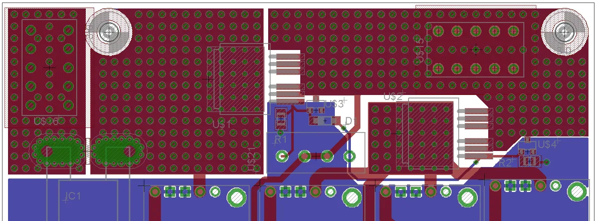
A PDN encompasses all conductive elements that supply power and ground to components, including planes, traces, vias, and decoupling capacitors. Power planes act as low-impedance reservoirs, distributing current efficiently while providing return paths for signals. Ground planes complement this by stabilizing reference potentials and reducing loop inductance. In multilayer boards, PDNs must handle transient currents from simultaneous switching without excessive voltage fluctuations. Poor PDN design manifests as voltage droop at IC power pins, causing timing errors or logic upsets.
The relevance of PDNs intensifies with rising clock speeds and core counts in processors. PCB power plane noise arises from high-frequency currents inducing voltage ripples across the plane. Excessive voltage drop starves components of required headroom, violating datasheet specifications and accelerating electromigration. Optimizing PDNs directly impacts compliance with signal integrity budgets and overall system margins. Engineers prioritizing PDN early in the design cycle avoid costly respins and ensure robust operation under worst-case scenarios.
Key Mechanisms Causing Noise and Voltage Drop
Voltage drop, or IR drop, occurs due to resistive losses in conductors carrying steady-state DC currents. The drop scales with current magnitude, conductor length, and resistivity, while inversely with cross-sectional area. In power planes, sheet resistance dominates for wide areas, but narrow traces or splits introduce higher localized drops. Transient voltage drops compound this during current spikes, demanding low-inductance paths. Accurate voltage drop calculation starts with estimating maximum currents per net and modeling resistance using sheet rho values derived from copper thickness and geometry.
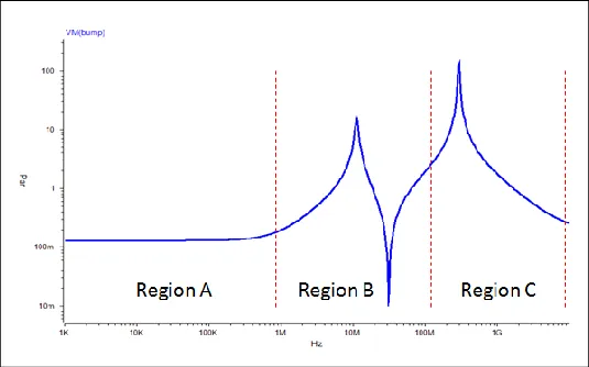
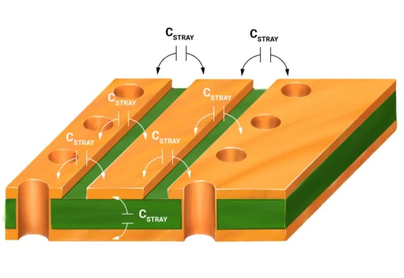
PCB power plane noise stems primarily from inductive and capacitive effects under dynamic loads. Fast edges from digital switching create high di/dt, generating voltage across plane inductance: V = L di/dt. Resonances between plane capacitance and inductance amplify noise at specific frequencies, often in the 10 MHz to 1 GHz range. Spreading inductance from distant return paths exacerbates this, coupling noise into signals. Cavity modes in parallel plane pairs further contribute to standing waves if unmitigated. Addressing these requires holistic analysis of PDN parasitics.
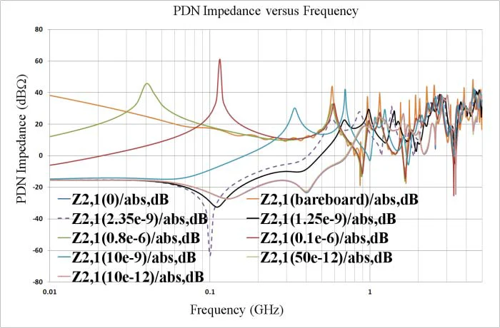
PDN impedance profiles reveal vulnerabilities across frequency spectra. DC resistance sets baseline drop, mid-range inductance controls transient response, and high-frequency capacitance determines ripple attenuation. Targets for PDN impedance aim for minimal peaks below component tolerances, typically flattening the curve through strategic capacitance. Simulations plot this impedance versus frequency, highlighting resonances for targeted fixes.
Establishing PDN Impedance Targets
Defining PDN impedance targets involves aligning with IC power supply ripple specs and noise margins. A practical target keeps impedance low enough so that maximum current times impedance yields voltage ripple within 5% of supply, though exact thresholds vary by design. Engineers calculate this by convolving load current spectra with impedance profiles. Plane pair separation influences capacitance, C = ε A / d, where closer planes boost capacitance but risk coupling. Wider planes reduce spreading resistance, aiding low DC impedance.
Achieving targets demands balanced layer stackups per IPC-2221B guidelines for conductor spacing and thickness. Adjacent power-ground pairs maximize capacitance while minimizing loop inductance. Via stitching along plane edges shorts resonances and equalizes potentials. Splitting planes for multiple rails requires careful partitioning to avoid high-impedance bridges. Iterative refinement ensures targets across DC to GHz ranges.
Practical Strategies for Minimizing Noise and Voltage Drop
Start with layout fundamentals: dedicate inner layers to solid power and ground planes, avoiding splits except where isolation is essential. Plane cuts for routing should include stitching vias every few millimeters to maintain low impedance. For voltage drop calculation, sum series resistances along current paths, incorporating temperature coefficients since resistivity rises with heat. Tools model this statically, but dynamic analysis captures peaks.
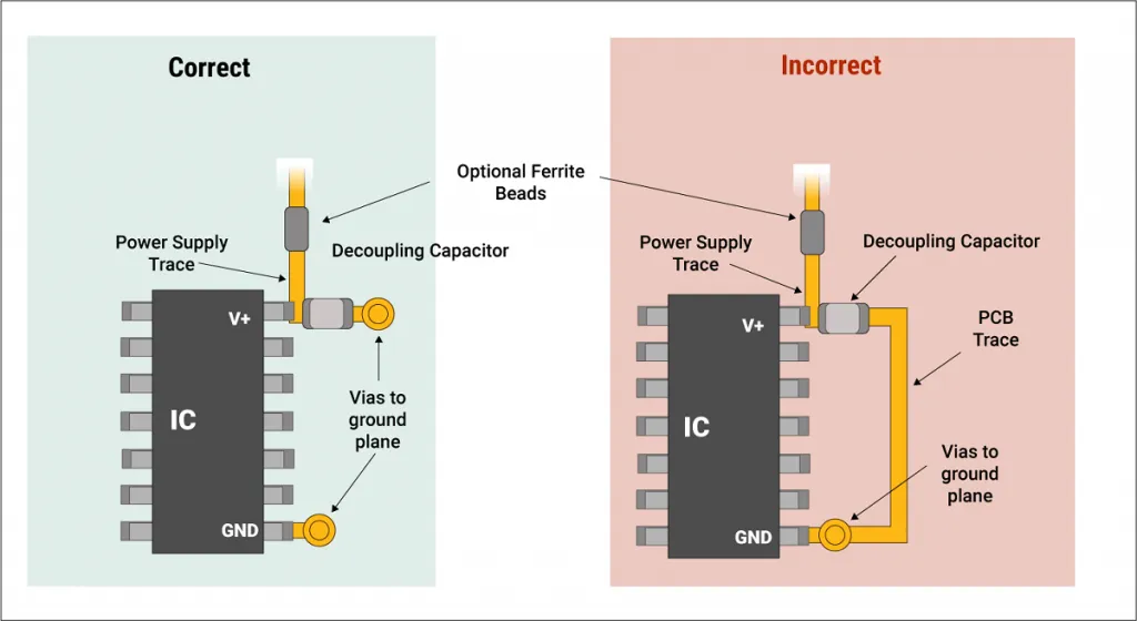
Decoupling capacitor selection critically covers the frequency spectrum. Bulk caps handle low frequencies with high capacitance values, while ceramic 0.1 μF types target mid-range, and smaller high-frequency caps suppress GHz noise. Criteria include low equivalent series inductance (ESL), self-resonance frequency (SRF) matching switching harmonics, and voltage rating exceeding supply. Place caps as close as possible to IC power pins, minimizing trace inductance. Arrays of varied values in parallel broaden coverage, with placement density guided by current slew rates.
Power distribution simulation verifies designs pre-layout and post. Time-domain transient analysis reveals voltage droops during load steps, while frequency-domain sweeps identify impedance targets. Hybrid models combine 2D field solvers for planes with 3D for components. Sensitivity studies optimize cap values and positions. Per J-STD-001 requirements for soldered assemblies, ensure cap terminations withstand thermal stresses without degrading PDN performance.
Advanced techniques include embedded capacitance layers for ultra-low inductance and active regulation for dynamic loads. Via-in-pad for high-density decoupling reduces parasitics. For noisy environments, guard traces around sensitive nets shield from plane noise.
Troubleshooting Common PDN Issues
Engineers often encounter excessive PCB power plane noise during validation, traced to insufficient decoupling or plane voids. Oscilloscope probes at power pins quantify ripple; FFT analysis pinpoints frequencies matching resonances. Voltage drop exceeding budgets signals undersized conductors, addressed by widening paths per IPC-2152A current capacity guidelines. Simulation discrepancies versus measurement highlight unmodeled parasitics like via inductance.
Mitigation workflows: resimulate with refined loads, add caps targeting peaks, then retest. Board-level fixes like extra vias prove effective for prototypes. Documenting PDN margins in design reviews prevents recurrence.
Conclusion
Optimizing PDNs demands integrated attention to layout, components, and verification. By mastering voltage drop calculation, pursuing PDN impedance targets, refining decoupling capacitor selection, and leveraging power distribution simulation, engineers minimize noise and ensure stability. Solid planes, strategic capacitance, and rigorous analysis form the core practices. Adhering to standards like IPC-2221B elevates designs from functional to exceptional. Implementing these steps yields reliable high-performance PCBs ready for production.
FAQs
Q1: How do you perform voltage drop calculation for PCB power planes?
A1: Voltage drop calculation involves estimating DC currents per net and computing IR losses along paths. Resistance derives from sheet resistivity, length, and width using formulas like R = ρ L / (W t). Factor in temperature rise for accuracy. Sum drops across segments to check against supply budgets. This static analysis guides conductor sizing before dynamic simulation.
Q2: What constitutes an effective PDN impedance target?
A2: A PDN impedance target maintains low, flat impedance across frequencies relevant to load transients, ensuring voltage ripple stays within IC tolerances. Profile DC resistance below milliohms, mid-range inductance under nH, and high-frequency capacitance for attenuation. Align with current spectra via simulation. Iterative tuning via decoupling achieves this.
Q3: How should engineers approach decoupling capacitor selection?
A3: Decoupling capacitor selection requires matching capacitance values and SRF to the switching current spectrum. Use bulk for low frequencies, mid-size ceramics for MHz, and small for GHz. Prioritize low ESL parts placed <1 mm from pins. Parallel combinations broaden coverage. Verify via PDN impedance profiles.
Q4: Why is power distribution simulation essential for PDNs?
A4: Power distribution simulation predicts noise and drops before fabrication, modeling parasitics across frequencies. It identifies resonances, optimizes cap placement, and validates impedance targets. Time and frequency analyses guide refinements. Without it, empirical fixes delay projects and risk failures. Essential for complex, high-speed boards.
References
IPC-2221B — Generic Standard on Printed Board Design. IPC, 2003
IPC-2152A — Standard for Determining Current Carrying Capacity in Printed Board Design. IPC, 2009
J-STD-001G — Requirements for Soldered Electrical and Electronic Assemblies. IPC, 2017