Introduction
Signal integrity challenges have become increasingly prominent in PCB design as operating frequencies rise and data rates climb into the gigahertz range. Engineers must address these issues starting from the schematic capture phase to ensure reliable performance in high-speed applications. Poor signal integrity in the PCB signal integrity schematic can lead to reflections, crosstalk, and electromagnetic interference that propagate through to layout and fabrication. By optimizing the schematic design for EMC and incorporating best practices for reducing noise in PCB schematics, designers can preempt many common pitfalls. This article explores structured approaches to high-speed PCB design schematics, emphasizing signal integrity analysis schematic techniques that align with industry standards. Ultimately, a well-crafted schematic lays the foundation for robust prototypes and production boards.
Understanding Signal Integrity in PCB Schematics
Signal integrity refers to the preservation of electrical signal quality from source to destination, free from distortion due to impedance mismatches, noise coupling, or timing errors. In the context of PCB schematics, it involves selecting components and topologies that minimize degradation before physical routing begins. Factors such as rise times, edge rates, and harmonic content determine when signal integrity becomes critical, often above 50 MHz for digital signals. Schematic flaws, like inadequate decoupling or missing terminations, amplify issues in layout, leading to eye diagram closure or bit error rates exceeding acceptable limits. Engineers must perform preliminary signal integrity analysis schematic reviews to identify risks early. Compliance with standards like IPC-2221A ensures foundational design principles support signal fidelity.
Crosstalk arises when aggressive signals couple into adjacent nets through capacitive or inductive mechanisms, a problem rooted in schematic proximity definitions. Ground bounce occurs from simultaneous switching noise on power rails, which schematics can mitigate through targeted decoupling strategies. Electromagnetic compatibility, or EMC, demands schematic provisions for filtering and shielding to meet regulatory thresholds. High-speed signals, such as those in DDR memory or PCIe interfaces, require differential pair definitions in the schematic to maintain balance and common-mode rejection. Neglecting these elements results in redesign iterations, increasing time to market. Thus, schematic design for EMC integrates noise reduction from the outset.
Key Technical Principles for Signal Integrity
Impedance control begins in the schematic by specifying characteristic impedances for critical nets, guiding later stackup and trace width decisions. Single-ended signals typically target 50 ohms, while differential pairs aim for 100 ohms differential impedance. Reflections occur when impedance discontinuities cause voltage waves to bounce back, degrading signal quality; schematics prevent this via termination networks. Series termination places a resistor equal to the source impedance at the driver output, absorbing reflections before they propagate. Parallel termination at the receiver matches the line impedance but draws more current. AC termination uses a resistor-capacitor series to ground, allowing high-frequency matching with DC savings.
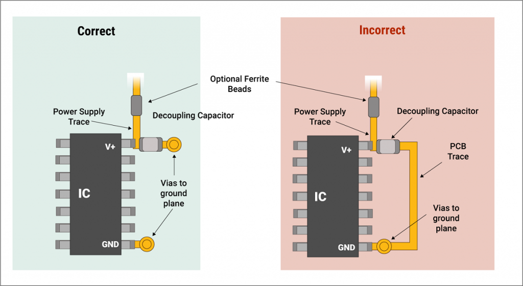
Power distribution network design in schematics ensures low-impedance paths for return currents, minimizing simultaneous switching noise. Bulk decoupling capacitors, around 10-100 uF, handle low-frequency demands near power inputs, while high-frequency ceramics, 0.1 uF or smaller, shunt noise at IC pins. Placement hierarchy in the schematic groups capacitors by function, facilitating layout proximity. Grounding schemes differentiate analog, digital, and noisy sections to avoid return path sharing. Star grounding converges currents at a single point, while planes offer distributed low inductance in multi-layer boards. These principles, drawn from IPC-2251 guidelines, address packaging for high-speed circuits.
Noise coupling mechanisms include capacitive crosstalk from overlapping electric fields and inductive from mutual flux linkage. Schematics reduce capacitive coupling by inserting guard traces or ground symbols between sensitive nets. Inductive coupling demands twisted pairs or shielding in analog sections. Clock distribution requires careful buffering to maintain edge integrity across fanouts. Pre-emphasis and equalization circuits compensate for losses, specified in schematics for serializer-deserializer links. Signal integrity analysis schematic simulations validate these choices before committing to layout.
Best Practices for Schematic Optimization
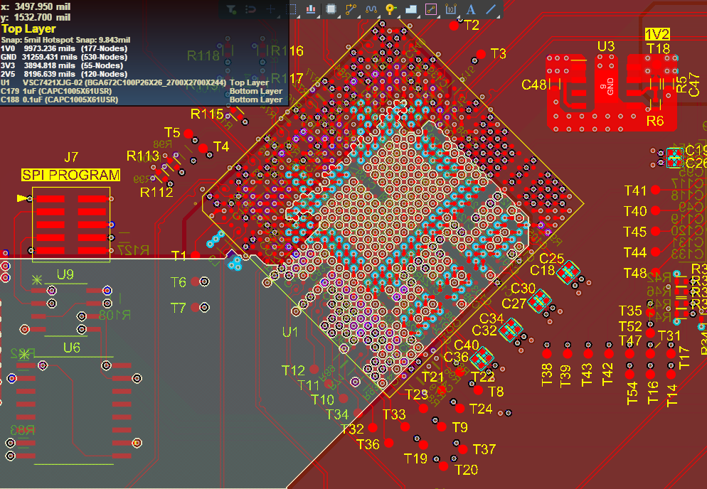
Start with hierarchical schematics to modularize high-speed sections, isolating critical paths for focused review. Define net classes for high-speed, default, and power nets, annotating impedance targets and length matching requirements. This PCB signal integrity schematic practice streamlines translation to layout tools. Incorporate termination resistors explicitly, calculating values based on driver output impedance and line characteristics. For source termination, place resistors within millimeters of the driver pin in the conceptual sheet. Verify differential pairs have symmetric routing cues, like length tolerances under 10 mils.
Decoupling strategy demands multiple capacitors per power pin, sized across frequency decades. Local 0.01 uF ceramics pair with 1 uF for mid-range, feeding from bulk storage. Ferrite beads on power lines suppress high-frequency noise without affecting DC. Schematic design for EMC includes RC filters on I/O lines to attenuate conducted emissions. Separate power domains with inductors or regulators to prevent cross-talk between voltage rails. Reducing noise in PCB schematics involves shielding sensitive analog inputs with op-amp guards tied to analog ground.
Specify bypass paths for ESD protection using TVS diodes on exposed pins, sized per threat levels. Clock trees benefit from zero-ohm jumpers or PLLs for clean distribution. Annotate schematics with SI notes, such as "Match lengths to <50 ps skew" or "50 ohm single-ended." Perform manual timing budgets in spreadsheets, summing propagation delays and setup/hold margins. Collaborate with layout engineers early via schematic reviews. These high-speed PCB design schematic techniques ensure manufacturability.
For multi-gigabit SerDes, include loop filters and bias tees as per protocol needs. Pre-layout IBIS modeling confirms driver-receptor compatibility. Guard against ground loops by single-point analog-digital ties. EMC filters on DC-DC converters use pi-networks of caps and inductors. Validate symmetry in balanced lines to preserve odd-mode impedance. These practices align with IEC guidelines for electromagnetic compatibility in circuit design.
Common Pitfalls and Troubleshooting Insights
Overlooking return current paths leads to elevated inductance and ringing, observable as overshoot in simulations. Insufficient decoupling causes voltage droop under load, triggering resets. Fanout exceeding buffer drive strength distorts edges; add redrivers proactively. Mismatched terminations reflect energy, closing eyes in high-speed links. Crosstalk from unshielded clocks couples into victims; isolate with ground planes implied in schematics.
Troubleshoot by scoping prototypes for anomalies, correlating back to schematic elements. Eye diagrams reveal jitter sources, often tracing to PDN impedance. TDR measurements confirm discontinuities missed in design. Iterative fixes include adding stubs or stubs. Preempt with signal integrity analysis schematic checklists.
Conclusion
Optimizing PCB schematic design for signal integrity demands foresight into layout realities and adherence to proven principles. From impedance matching and decoupling to EMC provisions, each choice compounds reliability. Implementing these best practices minimizes iterations and accelerates high-speed product deployment. Engineers benefit from structured reviews and modular designs. Ultimately, a robust PCB signal integrity schematic ensures performance margins in demanding applications.
FAQs
Q1: What are the main causes of poor signal integrity in PCB schematics?
A1: Poor PCB signal integrity schematic often stems from impedance mismatches, inadequate termination, and insufficient decoupling capacitors. Reflections from unterminated lines distort waveforms, while shared return paths amplify ground bounce. Crosstalk between proximate high-speed nets degrades margins. Early signal integrity analysis schematic identifies these, allowing fixes like series resistors or pi-filters before layout. Following IPC-2251 reduces such risks in high-speed designs.
Q2: How does schematic design impact EMC compliance?
A2: Schematic design for EMC integrates filters, shielding, and segregated grounds to suppress emissions and susceptibility. Placing ferrites and caps on power rails attenuates noise coupling. Differential signaling preserves balance against common-mode interference. Reducing noise in PCB schematic through domain isolation prevents conducted failures. Compliance testing validates these provisions per relevant standards.
Q3: What role does decoupling play in high-speed PCB design schematics?
A3: Decoupling in high-speed PCB design schematic shunts high-frequency noise, stabilizing supply voltages under switching transients. Multiple cap values cover broadband impedance minima. Proximity to pins minimizes ESL effects. Schematics specify hierarchies for layout adherence. This practice enhances eye quality and timing.
Q4: When should engineers perform signal integrity analysis on schematics?
A4: Signal integrity analysis schematic is essential during initial capture and after major changes, especially for nets above 200 MHz. Pre-layout checks confirm termination efficacy and PDN stability. Timing budgets verify hold/setup. High-risk protocols like USB3 demand it routinely. This proactive step avoids costly respins.
References
IPC-2221A — Generic Standard on Printed Board Design. IPC.
IPC-2251 — Design Guide for the Packaging of High Speed Electronic Circuits. IPC.


