Introduction
In high-speed PCB design, the stack-up configuration plays a pivotal role in ensuring reliable performance. As signal frequencies increase, issues like signal integrity degradation, impedance mismatches, and electromagnetic interference become prominent challenges. Proper stack-up optimization helps maintain controlled impedance and minimizes crosstalk, allowing signals to propagate with minimal distortion. Engineers must consider layer arrangement, dielectric thicknesses, and reference plane placement from the initial design phase. This guide explores key principles and best practices for achieving optimal stack-up in high-speed applications. By following structured approaches, designers can enhance overall board reliability and performance.
What Is PCB Stack-Up and Why It Matters for High-Speed Signals
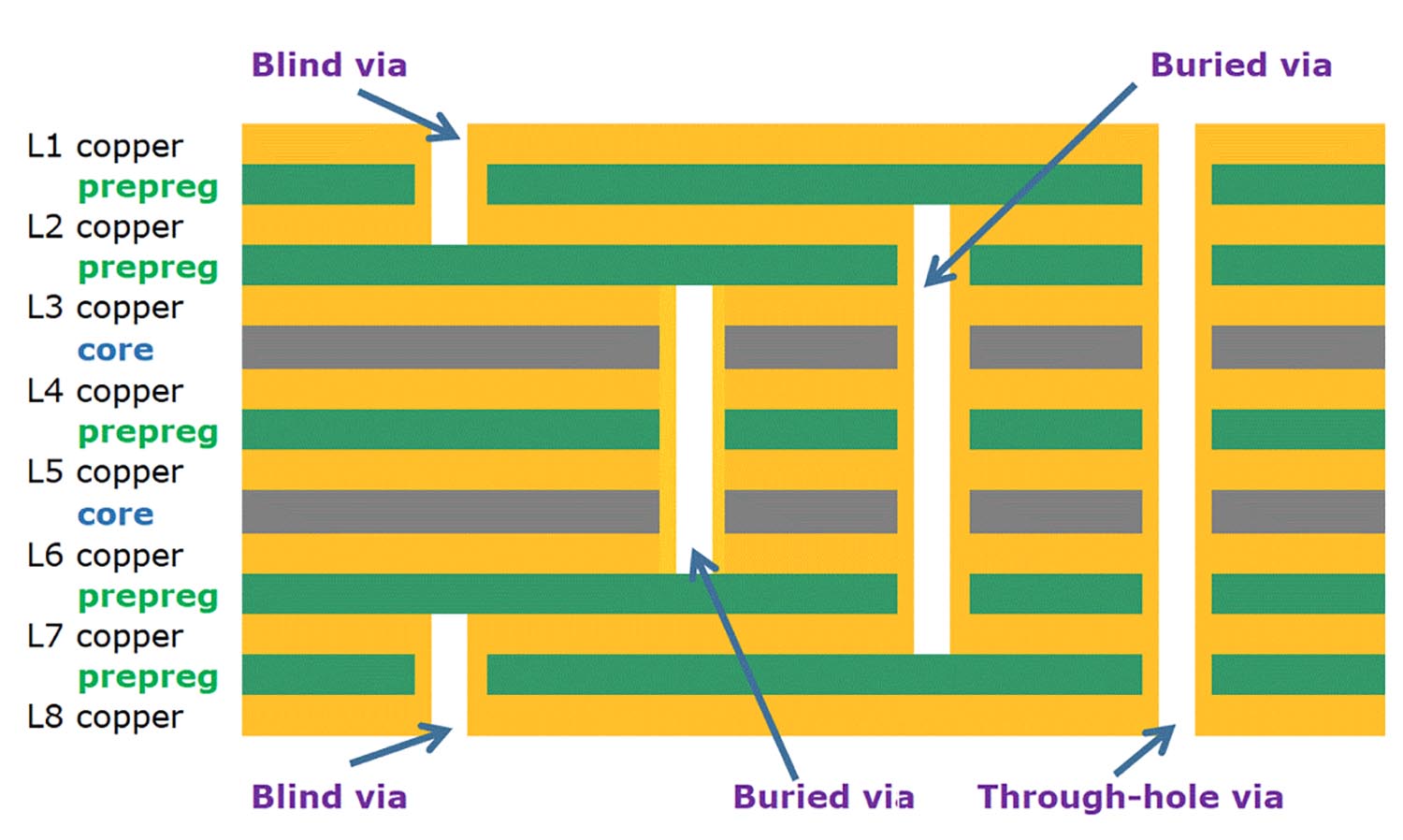
PCB stack-up refers to the specific arrangement of conductive layers, dielectrics, and cores in a multilayer board. It includes signal layers, power planes, ground planes, and insulating materials between them. In high-speed PCB design, stack-up directly influences transmission line characteristics and signal propagation. Poor stack-up can lead to uncontrolled impedance variations, increased insertion loss, and heightened sensitivity to manufacturing tolerances. Conversely, a well-planned stack-up supports signal integrity by providing consistent reference planes and symmetric structures.
The relevance intensifies with rising data rates in modern electronics, such as those in telecommunications and computing systems. High-speed signals demand precise control over characteristic impedance, typically 50 ohms or 100 ohms differential, to prevent reflections. Without optimization, crosstalk between adjacent traces compromises data integrity, while inadequate return paths elevate common-mode noise. Stack-up decisions also impact thermal management and mechanical stability, ensuring the board withstands fabrication and operational stresses. Ultimately, effective stack-up design aligns with industry requirements for robust high-speed performance.
Technical Principles of Stack-Up for High-Speed Signals
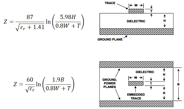
Transmission line theory forms the foundation of high-speed PCB stack-up design. Signals traveling along traces behave as guided waves, with impedance determined by trace geometry, dielectric constant, and proximity to reference planes. Microstrip configurations place traces on outer layers with air and dielectric above, while striplines embed traces between planes for better shielding. Controlled impedance requires balancing these parameters to match source and load impedances, reducing reflections as per basic wave equations. Variations in dielectric thickness or material properties can shift impedance by several ohms, necessitating tight tolerances.
Crosstalk reduction relies on minimizing capacitive and inductive coupling between traces. Forward crosstalk arises from mutual inductance, while backward crosstalk stems from capacitive coupling, both exacerbated in asymmetric stack-ups. Optimal spacing, often three times the trace width, coupled with ground planes, confines fields and lowers coupling coefficients. Reference planes provide low-inductance return paths, essential for high-frequency currents that follow the path of least impedance. Discontinuous planes or long via transitions disrupt these paths, increasing loop inductance and radiation.
Signal integrity further depends on plane capacitance and via optimization. Adjacent power and ground planes form distributed capacitors that decouple noise, stabilizing voltage rails. For high-speed signals, via stubs must be minimized through back-drilling or blind vias to avoid resonance. IPC-2221C outlines generic design parameters that support these principles, emphasizing layer sequencing for impedance stability. Dielectric materials with low loss tangents reduce attenuation at gigahertz frequencies, preserving eye diagram quality.
Return path optimization ensures current continuity, preventing ground bounce. High-speed signals induce return currents on the nearest reference plane, following image theory. Stitching vias around signal vias maintain short return loops, reducing inductance below 1 nH per via transition. Asymmetric stack-ups lead to warpage during lamination, altering dielectric spacing and impedance. Balanced core and prepreg thicknesses promote flatness, aligning with mechanical design goals.
Practical Solutions and Best Practices in Stack-Up Design
Begin stack-up planning by defining signal requirements, layer count, and impedance targets. Allocate dedicated signal layers adjacent to ground planes to form striplines, enhancing shielding and crosstalk reduction. For example, an 8-layer stack-up might sequence as signal-ground-power-signal-ground-signal-power-ground, providing multiple reference options. Simulate stack-up using field solvers to predict impedance and coupling before fabrication. Maintain dielectric thicknesses between 3 and 10 mils for fine-line control, adjusting trace widths accordingly.
Implement symmetry by mirroring layers around the neutral axis, mitigating warpage from CTE mismatches. Thin dielectrics between planes boost capacitance, aiding power integrity. IPC-2141A provides guidance on controlled impedance structures, recommending tolerances of plus or minus 10 percent initially, tightening to 5 percent for critical nets. Route high-speed signals on inner layers to avoid surface contamination effects on outer microstrips. Differential pairs benefit from tight coupling within the same layer, flanked by ground.
Address crosstalk through routing rules: separate high-speed nets by at least 3W spacing, where W is trace width, and use guard traces if needed. Optimize return paths with dense via stitching grids, spaced less than one-eighth wavelength at the highest frequency. Power plane cutouts should align with signal vias to preserve continuity. During design review, verify stack-up against fabrication capabilities, ensuring drill aspect ratios stay below 10:1.
For complex boards, hybrid stack-ups combine high-speed inner layers with low-speed outer layers. Pre-impregnated materials must match core expansion coefficients to prevent delamination. Final validation involves time-domain reflectometry post-fabrication to confirm impedance. These practices collectively ensure signal integrity in demanding environments.
Case Study: Optimizing an 8-Layer Stack-Up for DDR4 Signals
Consider a design with DDR4 memory interfaces operating above 3 GHz. Initial stack-up placed signals on outer layers without dedicated grounds, resulting in 15 percent impedance variation and measurable crosstalk. Redesign shifted signals to layers 3-6, sandwiching them between full ground planes on layers 2,4,7. Dielectric stacks used 1080 prepreg for thin cores, achieving 50-ohm single-ended impedance.
Crosstalk simulations showed a 20 dB improvement with 4W spacing and stitching vias every 500 mils. Return path inductance dropped below 0.5 nH, opening the eye diagram significantly. Symmetric construction eliminated 2 mils of warpage, maintaining tolerances. This adjustment aligned with high-speed PCB design goals, demonstrating practical gains from principled stack-up.
Conclusion
Optimizing PCB stack-up is essential for high-speed signals, directly impacting controlled impedance, signal integrity, crosstalk reduction, and return path efficiency. Logical layer sequencing, symmetric builds, and reference plane strategies form the core of effective designs. Adhering to established guidelines ensures manufacturability and performance. Engineers should iterate simulations early and validate prototypes rigorously. Mastering these elements elevates high-speed PCB design reliability across applications.
FAQs
Q1: What role does controlled impedance play in high-speed PCB design?
A1: Controlled impedance matches trace characteristics to driver and receiver specs, minimizing reflections that degrade signal integrity. In stack-up planning, precise dielectric thicknesses and plane proximity achieve target values like 50 ohms. Variations exceed 10 percent lead to overshoot and ringing. Proper control supports data rates beyond 10 Gbps effectively.
Q2: How can stack-up reduce crosstalk in high-speed signals?
A2: Stack-up reduces crosstalk by embedding signals between ground planes, confining electromagnetic fields. Maintain 3W minimum spacing between traces and use orthogonal routing on adjacent layers. Ground stitching vias further isolate aggressor and victim nets. This approach lowers coupling below -40 dB for most designs.
Q3: Why is return path optimization critical for signal integrity?
A3: Return paths provide low-impedance loops for high-frequency currents, preventing ground bounce and EMI. Continuous reference planes adjacent to signal layers ensure short paths. Via transitions without stitching increase inductance, distorting waveforms. Optimized paths maintain clean signals up to multi-GHz frequencies.
Q4: What are key best practices for high-speed PCB stack-up?
A4: Prioritize signal-ground adjacency, symmetric layering for warpage control, and thin dielectrics for capacitance. Simulate impedance early and specify tight tolerances. Avoid splitting planes under high-speed nets. These steps enhance overall signal integrity and reliability.
References
IPC-2221C — Generic Standard on Printed Board Design. IPC, 2023
IPC-2141A — Design Guide for High-Speed Controlled Impedance Circuit Structures. IPC, 2001
IPC-6012E — Qualification and Performance Specification for Rigid Printed Boards. IPC, 2017


