Introduction
Optimizing PCB stack-up for RF applications demands precise engineering to handle high-frequency signals effectively. In RF PCB design, the arrangement of conductive and dielectric layers directly influences signal propagation, minimizing losses and maintaining integrity. Engineers face challenges like dielectric losses, crosstalk, and mechanical stability, especially as frequencies climb into GHz ranges. This practical guide explores key principles and strategies for high-frequency stack-up, focusing on impedance matching, signal loss reduction, and seamless antenna design integration. By following structured approaches, designers can achieve reliable performance in demanding RF systems. The insights here draw from established engineering practices tailored for electric engineers.
What Is PCB Stack-Up and Why It Matters for RF Applications
PCB stack-up refers to the sequential layering of copper foils, cores, prepregs, and solder masks that form a multi-layer board. Each layer serves specific functions, such as signal routing, power distribution, or grounding, with dielectric thicknesses defining electrical characteristics. In RF applications, sigma-lta stack-up becomes critical because high-frequency signals interact strongly with material properties and geometries. Variations in dielectric constant or thickness can cause impedance discontinuities, leading to reflections and degraded performance. Proper stack-up ensures controlled impedance, reduces radiation emissions, and supports compact antenna design. Without optimization, issues like increased insertion loss or phase shifts compromise system efficiency.
High-frequency stack-up matters profoundly in modern RF systems, from wireless communications to radar modules. At frequencies above 1 GHz, skin effect confines currents to trace surfaces, amplifying the need for smooth copper and low-loss dielectrics. Asymmetric stack-ups induce warpage during fabrication or thermal cycling, misaligning vias and traces critical for RF paths. Optimized designs balance electrical performance with manufacturability, enabling higher data rates and longer range. For electric engineers, mastering stack-up translates to fewer iterations and faster time-to-market.
Key Technical Principles in High-Frequency Stack-Up Design
The foundation of high-frequency stack-up lies in dielectric materials with low dissipation factor (Df) and stable dielectric constant (Dk). Materials exhibiting Df below 0.005 at operating frequencies minimize signal loss by reducing energy conversion to heat. Core selection influences thickness uniformity, while prepregs fill gaps between layers, affecting overall impedance. Engineers must model field distributions to predict microstrip or stripline behavior accurately. Transmission line theory guides these choices, ensuring characteristic impedance aligns with system requirements.
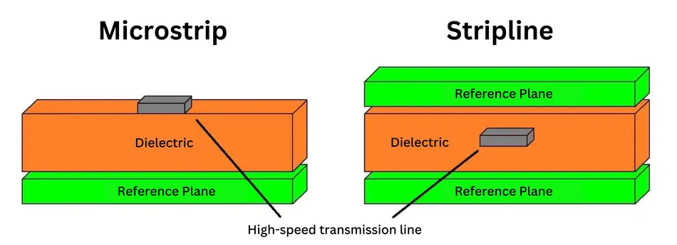
Impedance matching forms a core principle, governed by trace width, dielectric height, and surrounding planes. In microstrip configurations, signals propagate adjacent to air, offering simpler fabrication but higher radiation. Striplines, embedded between ground planes, provide better shielding at the cost of tighter tolerances. IPC-2221 outlines generic guidelines for section widths and spacings to control impedance across layers. Deviations lead to return loss, quantified as mismatches exceeding 10% of nominal 50 ohms.
Signal loss mechanisms include conductor loss from finite resistivity and dielectric loss from molecular friction. At high frequencies, these scale with sqrt(frequency), demanding thinner coppers or hybrid materials. Plane capacitance between power and ground layers stabilizes voltage, reducing noise coupling into RF traces. Symmetric stack-ups, with balanced core-prepreg pairs top-to-bottom, prevent bow and twist per mechanical stress models. Field solver simulations verify these interactions before fabrication.
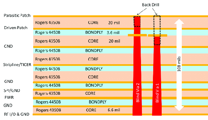
Crosstalk arises from mutual inductance and capacitance between adjacent traces, exacerbated in dense RF layouts. Ground planes act as return paths, confining fields and lowering coupling coefficients below -60 dB. Via transitions introduce stubs that reflect signals unless back-drilled or tuned. Antenna design integrates by dedicating outer layers for patches, with stack-up defining substrate height for resonance.
Practical Solutions and Best Practices for RF PCB Stack-Up Optimization
Start with layer count planning, favoring even numbers for symmetry in 4- to 12-layer boards common in RF. Assign signal layers adjacent to ground planes to shorten return paths and enhance isolation. Dedicate inner layers to power distribution with wide pours, minimizing inductance. Use thinner dielectrics between critical pairs to tighten impedance control within 5% tolerance. Fabricators can achieve this through laser-drilled blind vias and sequential lamination.
Material selection prioritizes low-loss laminates with Dk matching across layers to avoid intra-layer mismatches. Hybrid stack-ups combine standard cores with high-frequency prepregs where cost constrains full exotic builds. IPC-2228 specifies requirements for RF/microwave boards, emphasizing dimensional stability under thermal excursions. Verify stack-up via 3D field solvers early, iterating for target impedance and loss tangents.
Impedance matching employs coplanar waveguides or grounded coplanar for transitions, reducing discontinuities. Route RF traces straight, avoiding bends sharper than 45 degrees to preserve phase linearity. Minimize via count by fanning out signals horizontally before stitching grounds. For signal loss reduction, electropolish copper surfaces to below 1 micron roughness, cutting attenuation by 20% at 10 GHz.
Antenna design benefits from dedicated stack-ups with cavity substrates for patch arrays. Embed feeds using proximity coupling, tuning via layer spacing. Test prototypes with vector network analyzers to correlate models with reality. Maintain clearances per IPC-6012 performance specs to ensure qualification.
Common Challenges and Troubleshooting in RF Stack-Up
Warpage challenges symmetric designs during reflow, addressed by matching CTE across layers. Measure bow-twist post-lamination, targeting under 0.75% per IPC guidelines. Signal loss spikes from resin voids, detected via C-scan ultrasonics before assembly.
Crosstalk troubleshooting involves shielding vias along trace edges, achieving 20 dB isolation. Impedance drifts from plating thickness variations require fab specs under 0.5 mil control. Antenna detuning from nearby dielectrics demands guard rings or offsets.
Conclusion
Optimizing PCB stack-up for RF applications hinges on balancing electrical, mechanical, and manufacturing factors. Key strategies include symmetric layering, low-loss materials, and precise impedance control to curb signal loss and enable robust antenna design. Electric engineers benefit from iterative modeling and adherence to standards like IPC-2221, IPC-2228, and IPC-6012. Implementing these practices yields high-performance RF PCB designs with minimal revisions. Future trends toward mmWave will further emphasize hybrid materials and advanced simulations.
FAQs
Q1: What role does high-frequency stack-up play in RF PCB design?
A1: High-frequency stack-up defines signal paths, ground references, and dielectric environments critical for GHz operations. It ensures impedance matching by controlling layer thicknesses and material Dk/Df values. Poor stack-up amplifies signal loss through reflections and radiation. Engineers optimize it for minimal crosstalk and thermal stability. This directly impacts overall RF system efficiency and reliability.
Q2: How can engineers achieve impedance matching in RF PCB design?
A2: Impedance matching starts with trace geometry calculations using field solvers for target 50 ohms. Pair signals with adjacent ground planes to stabilize characteristic impedance. Select uniform dielectric heights across layers to avoid variations. Verify with time-domain reflectometry during prototyping. Consistent copper weights and surface finishes further refine matches.
Q3: Why is minimizing signal loss essential in high-frequency stack-up?
A3: Signal loss degrades RF performance by attenuating power and distorting waveforms at high frequencies. Dielectric and conductor losses compound with frequency, reducing range in wireless apps. Optimized stack-up uses low Df materials and smooth traces to cut attenuation. Ground stitching and return path minimization lower inductive losses. This preserves signal-to-noise ratios vital for antenna design.
Q4: What considerations apply to antenna design in RF PCB stack-ups?
A4: Antenna design requires stack-ups with precise substrate heights for resonance tuning. Outer layers host patches, backed by ground cavities for gain. Low-loss dielectrics prevent efficiency drops. Feed networks demand controlled impedance paths. Symmetry aids fabrication flatness, ensuring pattern integrity.
References
IPC-2221 — Generic Standard on Printed Board Design. IPC
IPC-2228 — Sectional Design Standard for High Frequency (RF)/Microwave Printed Boards. IPC
IPC-6012F — Qualification and Performance Specification for Rigid Printed Boards. IPC, 2023


