Introduction
In modern electronics, high-speed PCB designs operate at data rates exceeding several gigabits per second, making signal integrity PCB layout a critical factor for success. Poor signal integrity leads to issues such as bit errors, timing skew, and system failures, which can compromise overall performance. Advanced techniques in high-speed PCB routing, impedance control in PCB design, and crosstalk minimization techniques enable engineers to mitigate these challenges effectively. This article delves into structured approaches that electric engineers can implement to achieve robust signal transmission. By focusing on proven engineering principles, designers can ensure compliance with performance requirements in demanding applications like telecommunications and computing.
What Is Signal Integrity and Why It Matters in High-Speed PCBs
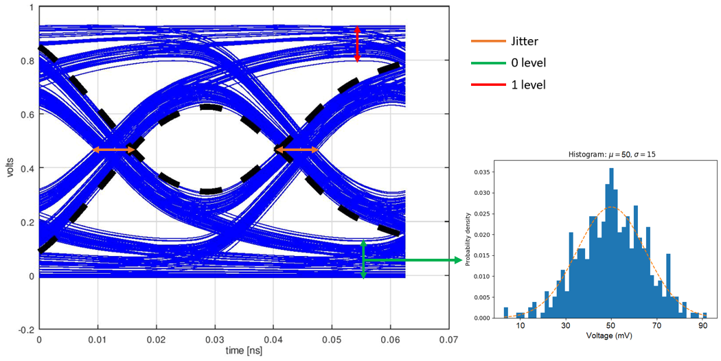
Signal integrity refers to the preservation of electrical signal quality from source to receiver, encompassing aspects like waveform shape, amplitude, and timing. In high-speed environments, signals behave as transmission lines where discontinuities cause reflections and distortions. Impedance mismatches, for instance, generate voltage reflections that degrade eye diagrams and increase jitter. Crosstalk between adjacent traces introduces noise, further complicating data recovery. For electric engineers, mastering signal integrity PCB layout is essential to meet rising frequency demands and maintain low bit error rates. Neglecting these factors results in costly redesigns and failed prototypes.
The relevance intensifies with shrinking process nodes and denser interconnects in multilayer boards. High-speed signals, often above 1 GHz, demand controlled environments to prevent attenuation and EMI radiation. Industry trends toward 5G, AI accelerators, and data centers amplify the need for precise layouts. Engineers must balance speed, density, and reliability, where even minor layout flaws propagate into system-level issues. Ultimately, strong signal integrity ensures interoperability and longevity in field deployments.
Fundamental Technical Principles Affecting Signal Integrity
Transmission line theory forms the backbone of signal integrity analysis, treating PCB traces as distributed RLC networks. Characteristic impedance, defined by trace geometry and dielectric properties, must remain constant to avoid reflections governed by the reflection coefficient formula. Dielectric materials influence propagation velocity and loss tangent, impacting signal attenuation over length. Skin effect confines current to trace surfaces at high frequencies, increasing effective resistance. Engineers calculate these parameters during stackup planning to predict behavior accurately. Understanding these mechanisms allows proactive design adjustments.
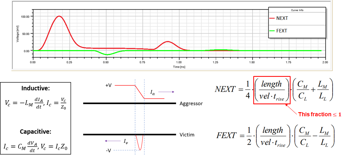
Crosstalk arises from capacitive and inductive coupling between aggressor and victim traces. Forward crosstalk shifts timing, while backward crosstalk induces common-mode noise. Ground bounce from simultaneous switching further couples noise into signals. Return path discontinuities, such as splits in reference planes, elevate inductance and exacerbate issues. Electric engineers quantify these through field solver simulations integrated into design flows. These principles guide layout decisions for optimal performance.
Advanced Impedance Control in PCB Design
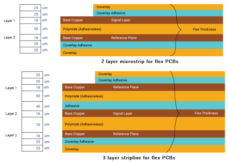
Impedance control in PCB design starts with meticulous layer stackup definition, specifying trace width, spacing, and dielectric thickness. Target impedances, typically 50 ohms single-ended or 100 ohms differential, require precise manufacturing tolerances. Varying copper weights and prepreg types fine-tune values without altering overall thickness. Engineers verify control using TDR measurements post-fabrication. Consistent impedance minimizes reflections, preserving signal edges. IPC-2221 provides foundational guidelines for conductor sizing and spacing to support these controls.
Reference planes adjacent to signal layers provide low-inductance return paths, stabilizing impedance. Partial ground fills or hatched planes serve in constrained areas but introduce variability. Via transitions demand stub minimization through backdrilling or blind vias to maintain continuity. Material selection favors low-loss dielectrics for frequencies above 10 GHz. Practical implementation involves iterative stackup optimization during early design phases. This approach ensures high-speed signals propagate with minimal distortion.
High-Speed PCB Routing Strategies
High-speed PCB routing prioritizes length matching for parallel buses to prevent skew, using serpentine or trombone patterns judiciously. Differential pairs route with constant spacing and orthogonal directions to adjacent signals, reducing loop area. Avoid 90-degree bends; use 45-degree or curved segments to minimize reflections. Minimize via count by aligning components and using microvias where feasible. Route critical nets first, reserving inner layers for shielding. These strategies form the core of effective signal integrity PCB layout.
Power and ground plane partitioning isolates noisy digital sections from sensitive analog traces. Dedicated high-speed layers flanked by planes enhance confinement. Clock signals demand symmetric routing to balance skew across receivers. Engineers employ length-tuning algorithms while respecting DRCs. Post-route verification confirms compliance through timing analysis. Such disciplined routing sustains multi-gigabit throughput reliably.
Crosstalk Minimization Techniques
Crosstalk minimization techniques emphasize trace separation exceeding three times the trace width for edge-coupled lines. Staggered vias and guard traces with grounded stitching interrupt coupling paths. Orthogonal routing between layers exploits field orientation differences. Increase dielectric thickness between aggressor-victim pairs in dense areas. Active shielding via driven guards cancels far-end crosstalk effectively. These methods integrate seamlessly into high-speed PCB routing workflows.
Far-end crosstalk dominates at high speeds due to velocity differences in coupling. Backward crosstalk mitigation involves solid reference planes without splits under traces. Frequency-domain analysis helps predict coupling coefficients. Engineers apply spacing rules scaled by edge rates. Combining spacing with shielding achieves over 20 dB isolation typically. Consistent application yields clean signals in congested boards.
Integrating Power Integrity with Signal Integrity
Power integrity couples tightly with signal integrity, as PDN impedance affects simultaneous switching noise. Decoupling capacitors placed near ICs provide local charge reservoirs. Plane resonance modes demand spread-spectrum clocking or targeted slits. Voltage droop analysis guides capacitor selection and placement. Engineers model PDN as parallel RLC networks for frequency response. Holistic consideration prevents SSO-induced jitter.
Via fences and moats partition power domains while maintaining return paths. Low-ESR ceramics in arrays handle high-frequency transients. Simulation correlates PDN impedance targets below 10 mOhm up to Nyquist frequency. Practical layouts balance density with margin. This synergy elevates overall board performance.
Best Practices for Implementation and Verification
Adopt a top-down design flow starting from system-level budgets down to trace-level rules. Collaborate across disciplines for stackup freeze early. Employ 3D field solvers for via and bend modeling. Prototype testing with VNA and oscilloscopes validates predictions. Iterate based on eye pattern closure margins. IPC-6012 outlines performance specs aligning with these verification steps.
Document routing constraints in a central rule deck. Review sessions catch DRC violations preemptively. Manufacturing DFM checks ensure fabricability of fine features. Field data from deployments refines future designs. Rigorous processes yield first-pass success rates.
Conclusion
Optimizing signal integrity in high-speed PCB layout demands a blend of theoretical understanding and practical execution. Key techniques like impedance control in PCB design, precise high-speed PCB routing, and crosstalk minimization techniques address core challenges effectively. Electric engineers benefit from structured approaches rooted in transmission line principles and reference plane strategies. Implementing these advanced methods ensures reliable operation at elevated speeds. Continuous verification solidifies design robustness against evolving demands.
FAQs
Q1: What are the primary causes of signal reflections in signal integrity PCB layout?
A1: Signal reflections primarily stem from impedance discontinuities at vias, bends, connectors, and terminations. Maintaining consistent characteristic impedance through controlled trace geometry and stackup mitigates these. Proper termination resistors match source or load impedances. Reference planes provide continuous return paths. Engineers prioritize smooth transitions to preserve waveform integrity in high-speed designs.
Q2: How does layer stackup impact impedance control in PCB design?
A2: Layer stackup dictates dielectric height, material constants, and copper thickness, directly influencing characteristic impedance. Symmetric builds around cores stabilize mechanical and electrical properties. Low-loss dielectrics reduce attenuation for gigabit signals. Engineers simulate variations to hit 50/100-ohm targets precisely. Manufacturing tolerances under 10% ensure repeatability.
Q3: What routing strategies minimize crosstalk in high-speed PCB routing?
A3: Key strategies include increasing trace spacing, orthogonal layer routing, and inserting grounded guard traces. Minimize parallel run lengths below coupling thresholds. Differential pairs with tight coupling reject common-mode noise. Solid planes shield between layers effectively. Verification through S-parameter analysis confirms isolation levels.
Q4: Why is reference plane integrity crucial for crosstalk minimization techniques?
A4: Reference planes offer low-impedance return paths, confining fields and reducing coupling to adjacent traces. Plane splits create high-inductance detours, amplifying noise. Stitching vias bridge gaps seamlessly. Engineers avoid routing over splits for critical nets. This practice enhances overall signal quality in dense layouts.
References
IPC-2221B — Generic Standard on Printed Board Design. IPC
IPC-6012E — Qualification and Performance Specification for Rigid Printed Boards. IPC
J-STD-001G — Requirements for Soldered Electrical and Electronic Assemblies. IPC


