Introduction
High-power PCB components, such as MOSFETs in power electronics applications, generate significant heat during operation. Effective thermal management prevents overheating, ensures reliability, and extends component lifespan. Thermal pads serve as critical interfaces between these components and the PCB, facilitating heat dissipation through conduction to copper planes and beyond. Poor thermal pad design leads to hotspots, reduced efficiency, and potential failure in high-current scenarios. Engineers must prioritize thermal pad design for MOSFETs to balance electrical performance with thermal efficiency. This guide explores principles, best practices, and optimization strategies for superior high current PCB thermal design.
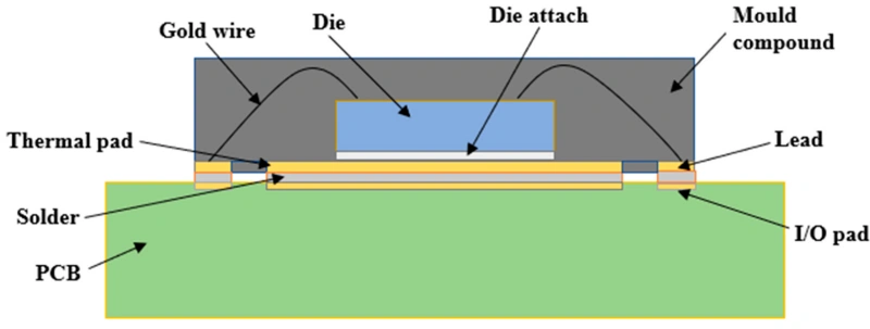
What Are Thermal Pads and Why Do They Matter in High-Power PCBs
Thermal pads are exposed metal areas on the bottom of surface-mount components like MOSFETs, designed specifically for heat transfer rather than electrical connection. In high-power applications, these pads connect directly to PCB copper areas to spread heat across the board. Without proper design, junction temperatures exceed safe limits, causing derating or failure. Industry standards like IPC-2221 emphasize thermal management in PCB layout to maintain performance under load. For electric engineers, optimizing thermal pads directly impacts system reliability in demanding environments such as power supplies and motor drives. High current PCB thermal design hinges on these pads to achieve uniform heat distribution.
The relevance grows with increasing power densities in modern electronics. Components handling tens of amps require robust heat paths to prevent thermal runaway. Thermal pads enable conduction to internal planes via thermal vias, enhancing overall dissipation. Neglecting this aspect results in inefficient cooling, even with external heatsinks. Engineers benefit from structured approaches to integrate thermal pads seamlessly into the layout process.
Related Reading: Beginner's Guide to Thermal Pads: Simple Steps for Effective Heat Dissipation
Fundamental Principles of Heat Transfer in Thermal Pads
Heat transfer from high-power components primarily occurs via conduction through the thermal pad to the PCB substrate. The thermal resistance depends on material properties, geometry, and contact quality. Copper's high thermal conductivity makes it ideal for pads and planes, minimizing temperature gradients. Convection and radiation play secondary roles unless augmented by airflow or heatsinks. Understanding Fourier's law guides design: heat flux is proportional to the temperature gradient and cross-sectional area, inversely to thickness.
In thermal pad design for MOSFETs, the pad acts as a heat spreader, converting point-source heat into planar flow. Effective designs lower theta-JA, the junction-to-ambient thermal resistance. Multi-layer boards leverage inner planes for additional spreading. Standards like IPC-2152 provide guidelines for current-carrying capacity, which correlates with thermal limits based on trace and plane heating. Engineers calculate paths using these principles to predict performance before prototyping.
Optimizing Thermal Pad Size: Guidelines and Considerations
Thermal pad size must match the component's exposed pad while extending for optimal spreading. Undersized pads concentrate heat, raising local temperatures. Oversizing improves dissipation but consumes board space and may complicate soldering. A conceptual thermal pad size calculator considers power dissipation, allowable temperature rise, and copper thickness to determine minimum area. High current PCB thermal design requires pads covering at least the component footprint, often extended by 1.5 to 2 times for better results.
Placement near board edges aids convection, but central locations suit symmetric airflow. Copper pour thickness influences size: thicker pours allow smaller pads due to lower resistance. Multi-layer pours stack for compounded effect. Engineers iterate sizes using simulation tools aligned with IPC guidelines to verify uniformity. Proper sizing prevents hotspots under parallel MOSFETs in phase-leg configurations.
Factors like board thickness and dielectric materials affect spreading angle. Thinner boards promote faster vertical conduction via vias. Engineers balance size with routing constraints for dense layouts.
Related Reading: The Ultimate Guide to Thermal Pad Materials: Choosing the Right One for Your Electronic Project
Thermal Pad Thickness for Optimal Heat Transfer
Thermal pad thickness refers to the copper foil weight on the PCB surface and planes connected to it. Thicker copper, such as 2 oz or more, reduces in-plane thermal resistance, enabling efficient radial spreading. However, manufacturing limits and cost increase with thickness. Optimal thermal pad thickness for optimal heat transfer balances conductivity with solderability and via reliability.
Heavier copper lowers theta-JC, the junction-to-case resistance path. In high-power designs, 1 oz suffices for moderate currents, while 3 oz or higher suits extreme cases. Plating adds minimal thickness but improves surface wetting. Engineers select based on total power and ambient conditions, verifying with thermal models.
Strategic Thermal Via Placement for Power Components
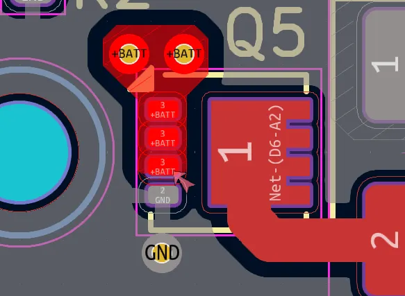
Thermal vias bridge surface pads to inner planes, creating vertical heat conduits. Placement directly under the pad periphery maximizes conduction without interfering with solder voids. Arrays of 0.3 mm to 0.5 mm vias, spaced 1 mm apart, provide low-resistance paths. Thermal via placement for power components follows a grid pattern, avoiding the pad center to preserve solder joint integrity.
Vias must connect all planes, stitched with solid fills for capacitance benefits. Tenting or filling prevents solder wicking during reflow. In high-density boards, staggered arrays enhance flow. Engineers position vias close to heat sources, ensuring at least 10-20 per pad for multi-watt devices. This setup complies with reliability standards for via thermal cycling.
Integrating Vias and Pads in Multi-Layer Designs
Multi-layer PCBs amplify thermal performance by stacking planes. Connect top thermal pad to bottom via mirrored pours. Use blind or buried vias for inner connections if through-vias overload. High current paths benefit from interleaved power-ground planes.
Simulation reveals via array efficacy, guiding density adjustments. Over-viaing risks board warpage; balance with copper balance rules.
Best Practices for High Current PCB Thermal Design
Start with component datasheets for theta-JC and recommended pad footprints. Extend copper pours across unused areas, stitching edges with vias. Employ heavier copper selectively under hot components. Maintain clearances for voltage isolation per IPC-2221.
Simulate early to iterate. Prototype with thermocouples for validation. Airflow direction influences pad orientation. Combine with heatsinks for hybrid cooling.
Common Challenges and Troubleshooting
Solder voids under pads trap heat, raising resistance. Minimize by reflow profiling per J-STD-020. Via plugging fails cause shorts; use filled vias. Warpage from asymmetric copper requires counterbalancing.
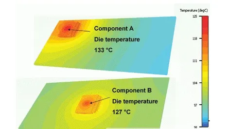
Hotspots from uneven via distribution demand redesign. Troubleshooting involves IR imaging to map flows.
Conclusion
Optimizing thermal pad design elevates high-power PCB reliability. Key elements include matched sizing, adequate thickness, and precise via placement. Adhering to principles ensures efficient heat transfer in demanding applications. Engineers achieve robust designs through systematic approaches.
FAQs
Q1: What factors determine thermal pad size for MOSFETs?
A1: Thermal pad design for MOSFETs depends on power dissipation, allowable temperature rise, and copper thickness. Extend beyond the component footprint for spreading. Use guidelines from IPC-2152 to estimate minimum area. Simulation refines size for specific layouts. Balance with board space constraints.
Q2: How do I calculate optimal thermal pad thickness?
A2: Thermal pad thickness for optimal heat transfer scales with current demands. Thicker copper reduces resistance but increases cost. Select 1-3 oz based on total heat load. Verify with thermal models. Multi-layer stacking enhances effectiveness.
Q3: Where should thermal vias be placed for power components?
A3: Thermal via placement for power components centers on pad edges in arrays. Space closely under high-heat areas. Connect to all planes. Avoid centers to protect solder joints. This lowers thermal resistance significantly.
Q4: What role does high current PCB thermal design play in MOSFET reliability?
A4: High current PCB thermal design prevents overheating in MOSFETs via robust pads and vias. Uniform heat spreading avoids derating. Follow standards for current capacity. Proper design extends operational life.
References
IPC-2221B - Generic Standard on Printed Board Design. IPC, 2012
IPC-2152B - Standard for Determining Current Carrying Capacity in Printed Board Design. IPC, 2009
IPC-6012E - Qualification and Performance Specification for Rigid Printed Boards. IPC, 2017