Introduction
Printed Circuit Board (PCB) design is a foundational skill for electronic hobbyists eager to bring their ideas to life. Whether you are crafting a simple LED circuit or a complex microcontroller project, understanding PCB design transforms concepts into functional devices. This guide introduces beginners to the essentials of creating circuit boards, focusing on key elements like electrical signals, copper traces, and user-friendly software tools. With a structured approach, you can navigate the process of designing a PCB using easy EDA platforms and grasp the principles behind reliable layouts. The goal is to equip you with practical knowledge to start designing boards that meet your project needs while adhering to industry best practices. Let’s explore the fundamental concepts and actionable steps to kickstart your journey into PCB design.
What Is PCB Design and Why It Matters
PCB design involves creating a layout for a printed circuit board that connects electronic components through conductive pathways, often made of copper traces. These boards serve as the backbone of most electronic devices, providing both mechanical support and electrical connectivity. For hobbyists, mastering PCB design means moving beyond temporary breadboard setups to permanent, compact, and efficient solutions.
The importance of PCB design lies in its impact on functionality and reliability. A well-designed board ensures that electrical signals flow correctly without interference, minimizing issues like noise or short circuits. Poor design, on the other hand, can lead to failures, overheating, or erratic performance. For beginners, learning this skill opens doors to custom projects, from home automation gadgets to wearable tech, while fostering a deeper understanding of electronics. As circuit boards are central to modern technology, the ability to design them is a valuable asset in any hobbyist’s toolkit.
Technical Principles of PCB Design
Understanding Circuit Boards and Components
At its core, a PCB is a flat board made of insulating material, typically fiberglass, with conductive copper traces etched onto its surface. These traces act as wires, connecting components like resistors, capacitors, and integrated circuits. Beginners must first understand how components interact on a board. Each part has a specific role, and their placement affects how electrical signals travel. Proper spacing prevents interference, while correct orientation ensures functionality.
The design process starts with a schematic, a diagram showing how components connect logically. This blueprint is then translated into a physical layout, where actual positions and copper pathways are defined. Standards like IPC-2221B, which outlines generic design principles for printed boards, emphasize the need for clear documentation at this stage to avoid errors during manufacturing.
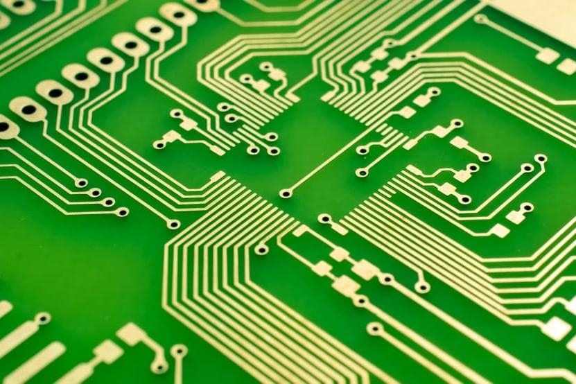
Role of Copper Traces in Signal Transmission
Copper traces are the conductive lines on a PCB that carry electrical signals between components. Their width, thickness, and placement directly influence performance. Narrow traces can handle less current and may overheat, while wide traces reduce resistance but take up more space. For hobbyists, balancing trace size with board constraints is critical.
Electrical signals traveling through copper traces can face issues like crosstalk or signal loss if traces are too close or improperly routed. Following guidelines from standards such as IPC-2222A, which covers sectional design for rigid organic printed boards, helps in determining appropriate trace spacing and width based on current and voltage needs. Beginners should prioritize straight, short traces to minimize delays and avoid sharp corners that can disrupt signal integrity.
Layers and Stackup Basics
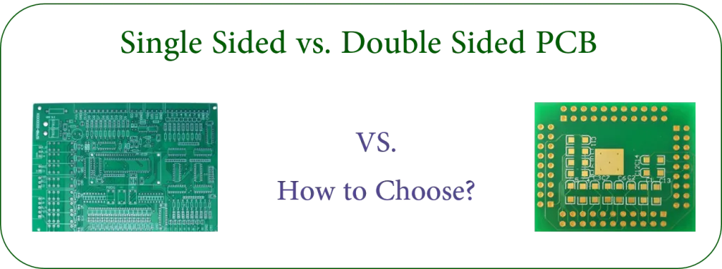
PCBs can have multiple layers, each with its own set of copper traces. Single-layer boards are simplest for beginners, with traces on one side only. Double-layer boards, with traces on both sides, offer more routing options for complex designs. Multi-layer boards, often used in advanced projects, stack several layers to save space and improve performance.
The arrangement of these layers, known as stackup, affects signal quality and electromagnetic interference. Even for simple projects, understanding stackup basics ensures better planning. Referencing IPC-6012E, a standard for qualification and performance of rigid printed boards, provides insight into layer configurations that maintain structural integrity and signal reliability.
Related Reading: Multilayer PCB Design for Beginners: A Step by Step Guide to Creating Your First Multilayer Board
Practical Steps for PCB Design with Easy EDA Tools
Step 1: Choose the Right Software
For beginners, selecting user-friendly electronic design automation (EDA) software is essential. Easy EDA tools offer intuitive interfaces and often run directly in web browsers, eliminating the need for powerful hardware. These platforms typically include schematic editors, layout tools, and simulation features to test designs before manufacturing. Look for software with extensive component libraries and community support to simplify the learning curve.
Step 2: Create a Schematic
Start by drawing a schematic that maps out your circuit. Place components and draw connections to represent how electrical signals flow. Ensure every component is labeled clearly, and double-check connections against your project requirements. This step is crucial as errors here will carry over to the physical layout. Standards like IPC-7351B, which addresses land pattern design for surface mount components, can guide component placement even at the schematic stage.
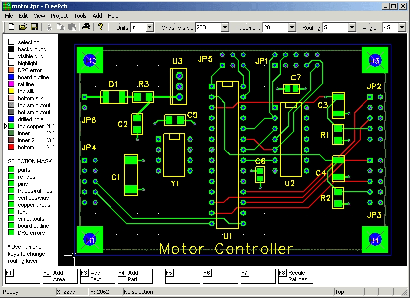
Step 3: Design the Layout
Once the schematic is complete, transition to the layout phase. Import the schematic into the layout editor, where components are placed on a virtual board. Arrange them to minimize the length of copper traces while avoiding overlap. Route traces to connect components, keeping power and ground lines separate to reduce noise. Pay attention to spacing rules outlined in IPC-2221B to prevent electrical interference.
Step 4: Validate and Simulate
Most easy EDA tools allow design rule checks to spot errors like unconnected traces or spacing violations. Run these checks to ensure compliance with basic design standards. If the software offers simulation, test how electrical signals behave in your circuit. This step helps identify potential issues like voltage drops or signal delays before moving to production.
Step 5: Generate Manufacturing Files
After finalizing the design, export files needed for manufacturing, often in a format specified by industry standards. These files include the layout, drill holes, and layer information. Review them to confirm all elements are correct. Following guidelines from IPC-A-600K, which sets acceptability criteria for printed boards, ensures your design meets manufacturing expectations.
Common Challenges and Best Practices
Avoiding Signal Interference
One frequent issue for beginners is signal interference caused by poorly routed copper traces. High-speed electrical signals can induce noise in nearby traces if not managed properly. Keep sensitive traces away from power lines and use ground planes to shield signals. Refer to IPC-2222A for spacing recommendations that minimize crosstalk in your circuit boards.
Managing Heat Dissipation
Components on a PCB generate heat, and improper design can lead to overheating. Place heat-generating parts with adequate spacing and consider adding vias to transfer heat between layers. Copper pours, large areas of copper connected to ground or power, can also aid in heat distribution. Standards like IPC-6012E provide criteria for thermal management in rigid boards.
Related Reading: A Beginner's Guide to PCB Thermal Design.
Testing Before Production
Always prototype and test your design on a small scale if possible. Use a multimeter to check continuity of copper traces and verify that electrical signals reach intended destinations. Simulation within easy EDA software can predict performance, but physical testing confirms real-world behavior. This approach aligns with best practices in IPC-A-600K for ensuring board quality.
Conclusion
PCB design is an accessible yet powerful skill for electronic hobbyists ready to elevate their projects. By understanding the role of circuit boards, copper traces, and electrical signals, beginners can create functional and reliable designs. Using easy EDA software simplifies the process, offering tools to draw schematics, route traces, and validate layouts. Following industry standards ensures that designs are manufacturable and perform as expected. With practice and attention to detail, hobbyists can tackle increasingly complex projects, turning ideas into tangible electronics. Start small, learn the principles, and build your confidence in crafting custom PCBs.
FAQs
Q1: What is PCB design, and why should hobbyists learn it?
A1: PCB design is the process of creating layouts for printed circuit boards that connect electronic components. For hobbyists, learning this skill allows the creation of permanent, compact circuits instead of temporary breadboard setups. It enhances project reliability and opens opportunities for custom electronics like sensors or gadgets, providing a deeper understanding of how electrical signals work.
Q2: How do copper traces affect circuit board performance?
A2: Copper traces are conductive pathways on circuit boards that carry electrical signals. Their width and placement impact current capacity and signal quality. Narrow traces may overheat, while poor routing can cause interference. Proper design, following industry spacing guidelines, ensures signals travel efficiently without noise or loss, maintaining overall performance.
Q3: Which easy EDA software is best for beginners in PCB design?
A3: Many easy EDA tools are suitable for beginners due to their intuitive interfaces and web-based access. Look for software with schematic editors, layout tools, and community support. Features like design rule checks and simulation help catch errors early. Exploring different platforms can help find one that matches your project needs.
Q4: How can I ensure electrical signals are reliable on my PCB?
A4: To ensure reliable electrical signals, route copper traces with minimal length and avoid sharp bends. Separate power and signal lines to prevent interference, and use ground planes for shielding. Validate your design with simulation tools in EDA software and adhere to spacing standards to minimize crosstalk and signal loss.
References
IPC-2221B — Generic Standard on Printed Board Design. IPC, 2012.
IPC-2222A — Sectional Design Standard for Rigid Organic Printed Boards. IPC, 2010.
IPC-6012E — Qualification and Performance Specification for Rigid Printed Boards. IPC, 2020.
IPC-A-600K — Acceptability of Printed Boards. IPC, 2020.
IPC-7351B — Generic Requirements for Surface Mount Design and Land Pattern Standard. IPC, 2010.


