Introduction
In modern PCB design, ground planes serve as the backbone for signal integrity and electromagnetic compatibility. As circuits grow more complex with mixed analog and digital signals, engineers often consider splitting the ground plane to isolate noisy digital sections from sensitive analog components. PCB ground plane splits can enhance performance in mixed-signal PCB design, but they introduce risks like unintended radiation or ground bounce if implemented poorly. Understanding when to use these splits, along with their pros and cons, helps prevent costly redesigns and failures. This article explores the principles behind split ground planes, best practices for their application, and strategies to avoid common pitfalls. By following structured engineering approaches, designers can leverage splits effectively while maintaining reliability.
What Are PCB Ground Plane Splits and Why Do They Matter?
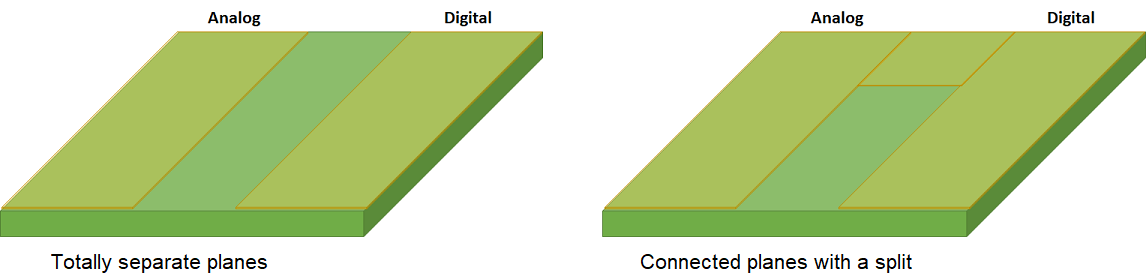
A PCB ground plane split divides a continuous copper pour into separate regions, typically for analog ground and digital ground separation. In mixed-signal PCB design, digital circuits generate high-frequency switching noise that can couple into analog paths through a shared ground plane, degrading signal-to-noise ratios. Splitting the plane creates isolated return paths, minimizing this crosstalk and improving overall system performance. However, this technique matters because improper splits can create high-impedance paths or radiating slots, exacerbating issues like electromagnetic interference.
The relevance stems from the increasing integration of analog sensors, amplifiers, and data converters alongside microcontrollers and high-speed logic. Without splits, ground bounce from simultaneous digital switching induces voltage fluctuations across the plane, affecting precision analog measurements. Industry practices emphasize careful planning to balance isolation benefits against potential discontinuities. For electric engineers, mastering PCB ground plane splits ensures compliance with signal integrity requirements in applications from audio processing to RF modules.
Technical Principles Behind Ground Plane Splits
Ground planes provide low-impedance return paths for currents, reducing inductive loops that amplify noise. In a solid plane, digital return currents spread out evenly, but their proximity to analog signals allows noise coupling via capacitive and inductive parasitics. Splitting the plane assigns dedicated areas: digital ground handles high di/dt transients, while analog ground preserves low-noise integrity. This separation aligns with analog ground vs digital ground principles, where return paths stay local to their signal domains.
Ground bounce occurs when multiple digital outputs switch simultaneously, causing transient currents to elevate ground potential through plane inductance. The effect worsens with faster edges and higher pin counts, manifesting as ringing or jitter in analog outputs. Splits mitigate this by confining digital currents away from analog vias and traces. Yet, the slot between splits acts as a slot antenna if longer than a wavelength fraction, radiating energy and violating EMC limits.
Current flow follows the path of least impedance, so splits force digital returns to stay in their region unless bridged incorrectly. Engineers must model these behaviors using field solvers to predict coupling levels. Parasitic capacitance across the split remains, though minimized by physical separation. Adhering to IPC-2221 guidelines for plane design helps quantify minimum split widths based on frequency content.
Split Ground Plane Pros and Cons in Practice
The primary pro of split ground planes lies in superior noise isolation for mixed-signal PCB design. By segregating analog ground vs digital ground, splits reduce common-mode noise by orders of magnitude, enabling cleaner ADC readings or DAC outputs. They also simplify EMC compliance, as digital noise stays contained, easing shielding needs. In high-density boards, splits allow optimized via placement without compromising returns.
However, cons include increased design complexity and potential for errors. Slots introduce discontinuities that demand stitching vias or capacitors to equalize potentials at high frequencies. Traces crossing splits without bridges pick up slot-mode currents, injecting noise. Manufacturing tolerances per IPC-6012E can widen splits unintentionally, raising impedance.
Another drawback is thermal management challenges, as splits fragment heat-spreading copper. Pros outweigh cons in precision applications like medical devices or instrumentation, but single planes suffice for purely digital or low-speed mixed boards. Weighing split ground plane pros and cons requires simulating worst-case current distributions.
When to Use PCB Ground Plane Splits
Use splits when analog sections demand sub-microvolt noise floors amid gigahertz digital clocks. Thresholds include digital edges faster than 100 MHz or ADCs with ENOB above 12 bits. In RF-mixed designs, splits prevent LO leakage into baseband. Avoid splits in low-frequency or power-dominated boards, where a single plane offers better thermal and mechanical stability.
Evaluate based on noise budget: if simulations show >1% THD from coupling, splits become necessary. Multi-layer stacks with dedicated analog planes reduce split needs. For cost-sensitive volumes, single-plane moats or guard traces often suffice as compromises.
Best Practices for Implementing Split Ground Planes
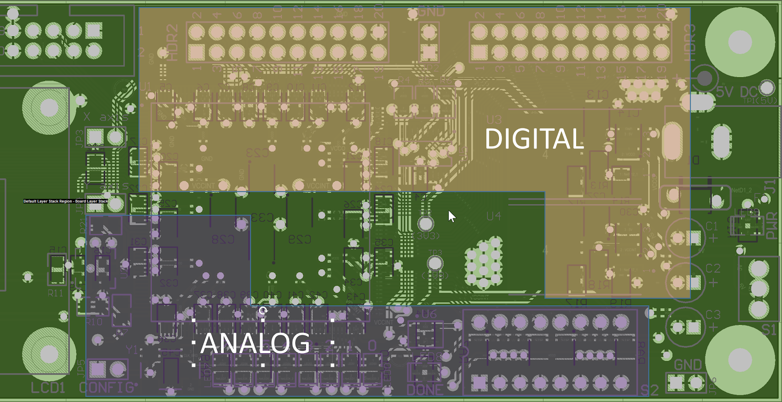
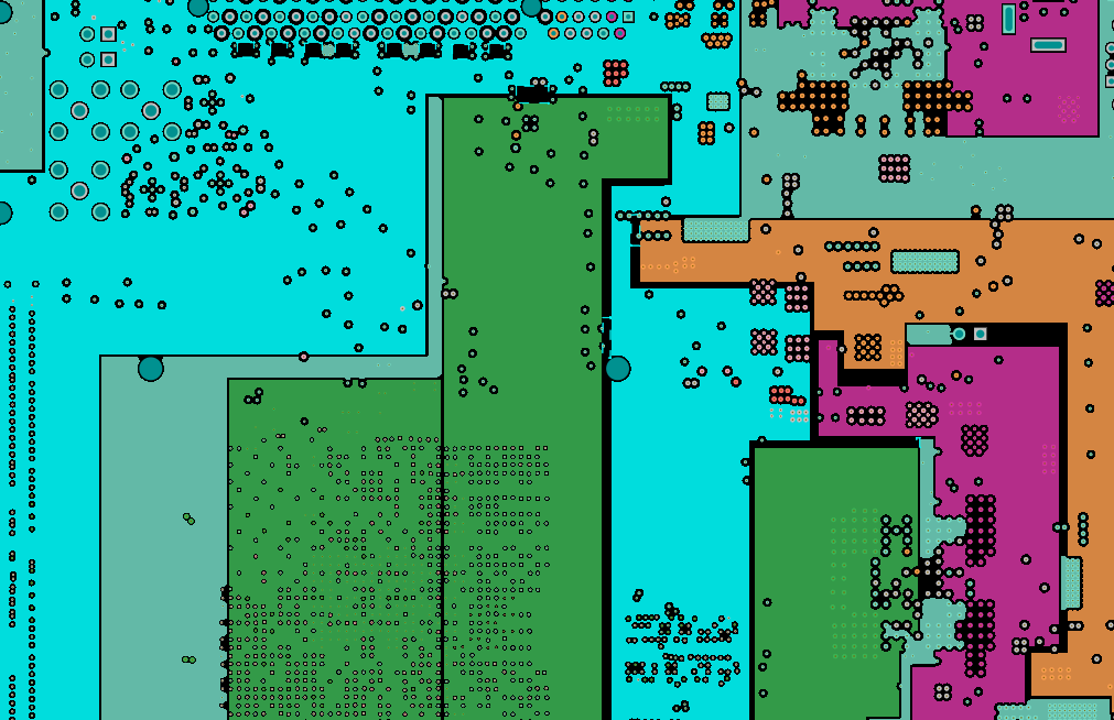
Start with layer stackup planning, dedicating inner layers for analog and digital grounds. Maintain split gaps of 3-5 times the highest frequency wavelength divided by 300, ensuring no resonance. Place components so analog pins connect only to analog ground, digital to digital. Use dense stitching vias along split edges, spaced at lambda/20, connected by 0.1uF capacitors for AC bridging.
Route no signals across splits; if unavoidable, use differential pairs with balanced guards. Connect splits at a single low-impedance point near power entry, forming a star topology. Simulate with 3D field tools to verify < -60dB coupling. Follow J-STD-001 for via reliability under thermal stress.
Guard rings around sensitive analog areas further isolate noise. Power planes should mirror ground splits to avoid slot coupling there too. Prototype testing with near-field probes validates isolation before production.
Common disasters arise from overlooked return paths: digital currents leaping splits via bond wires cause ground bounce spikes. Undersized stitches fail at GHz, opening slots. Overly narrow gaps couple capacitively. Mitigate by iterative PDN analysis.
Troubleshooting Ground Plane Split Issues
Engineers facing erratic analog performance post-split suspect improper current sharing. Probe ground potentials across domains; deltas >50mV indicate bridging failures. EMI scans reveal slot radiation peaks. Solutions include adding ferrite beads on bridges or repartitioning components.
In high-power cases, thermal vias in splits prevent hotspots. If ground bounce persists, reduce simultaneous switching via clock staggering. Documentation of split rationale aids design reviews.
Conclusion
PCB ground plane splits offer powerful isolation in mixed-signal PCB design but demand precision to avoid ground bounce and radiation pitfalls. Balancing split ground plane pros and cons through simulation and standards like IPC-2221 ensures success. Key takeaways include strategic stitching, local returns, and thorough verification. Electric engineers who apply these practices achieve robust, compliant designs. Prioritize splits judiciously, favoring single planes where isolation suffices. This approach minimizes disasters while maximizing performance.
FAQs
Q1: What are PCB ground plane splits and when should electric engineers use them?
A1: PCB ground plane splits divide the ground pour into analog and digital regions to prevent noise coupling in mixed-signal PCB design. Use them when digital switching noise threatens analog accuracy, such as in high-resolution data acquisition. Single planes work for low-speed circuits. Always simulate coupling first to confirm need, following structured layout rules for isolation.
Q2: What are the split ground plane pros and cons in analog ground vs digital ground separation?
A2: Pros include reduced crosstalk and easier EMC compliance, vital for precision analog. Cons involve slot radiation risks and added complexity from stitching. Proper implementation tips the balance toward pros. Weigh against board constraints before deciding.
Q3: How can ground bounce be mitigated in PCBs with ground plane splits?
A3: Ground bounce from digital switching worsens without splits but persists if bridges fail. Mitigate with dense stitching vias, capacitors, and local decoupling. Ensure no traces cross splits. Testing confirms <10mV peaks.
Q4: What common mistakes lead to disasters in PCB ground plane splits?
A4: Mistakes include narrow gaps causing capacitive coupling or missing AC bridges allowing high-frequency paths. Currents jumping domains induce noise. Avoid by modeling PDN impedance and prototyping.
References
IPC-2221G — Generic Standard on Printed Board Design. IPC, 2017
IPC-6012E — Qualification and Performance Specification for Rigid Printed Boards. IPC, 2018
J-STD-001H — Requirements for Soldered Electrical and Electronic Assemblies. IPC, 2020


