Introduction
In PCB stack-up design, the placement and configuration of ground planes play a critical role in ensuring signal integrity, electromagnetic compatibility, and overall board performance. Engineers designing multilayer PCBs must carefully consider ground plane layer stack-up to minimize crosstalk, control impedance, and provide low-impedance return paths for high-speed signals. Poorly configured ground planes can lead to increased EMI radiation, signal reflections, and thermal issues that compromise reliability. This article explores the principles behind effective ground plane configurations, best practices for various layer counts, and strategies for high-speed stack-up optimization. By understanding these elements, electrical engineers can select the right setup for their specific application requirements. Proper ground plane integration aligns with industry standards like IPC-2221, which provides foundational guidelines for printed board design.
What Is PCB Ground Plane Stack-Up and Why It Matters
A PCB ground plane stack-up refers to the strategic arrangement of copper ground layers within the overall multilayer PCB design. These planes serve as a common reference for signal return currents, shielding sensitive traces from external noise, and distributing heat evenly across the board. In high-speed stack-up configurations, ground planes are essential for maintaining characteristic impedance and reducing loop inductance. Without dedicated ground planes, signals propagate with unpredictable behavior, leading to timing skews and data errors in digital circuits. The relevance grows in modern designs handling gigabit data rates, where even minor impedance variations can degrade performance. Effective ground plane layer stack-up directly impacts manufacturability, as it influences warpage control and plating uniformity during fabrication.
Engineers prioritize ground planes in impedance control stack-up to achieve predictable transmission line behavior. A continuous ground plane adjacent to signal layers forms a stripline or microstrip structure, enabling tight coupling and low radiation. This setup complies with performance specifications in IPC-6012E, ensuring rigid printed boards meet qualification criteria for multilayer constructions. Neglecting proper stack-up can result in field imbalances that couple noise between layers, complicating EMI compliance. Thus, ground plane configuration is a foundational decision in PCB stack-up design, balancing electrical, mechanical, and thermal demands.
Technical Principles of Ground Plane Placement
Ground planes function primarily as return paths for currents induced by signal traces, following the principle that return currents mirror signal paths in the lowest impedance route. In multilayer PCB design, placing a ground plane immediately below the top signal layer minimizes the loop area, reducing inductive coupling and EMI emissions. This adjacency creates a controlled dielectric environment, where the trace-to-plane spacing dictates the effective impedance. For instance, thinner dielectrics between signal and ground enhance coupling but require precise material selection to avoid fabrication tolerances issues. Engineers must also consider plane capacitance, which provides decoupling for high-frequency noise when paired with nearby power planes.
Symmetry in ground plane layer stack-up prevents mechanical stress during lamination, as asymmetric configurations lead to differential shrinkage and board warpage. Core and prepreg thicknesses play a key role, with ground planes often positioned on inner layers to shield outer signals. In high-speed applications, multiple ground planes distribute return currents efficiently, avoiding bottlenecks at vias. Voids or splits in ground planes disrupt current flow, forcing detours that increase inductance and radiate noise. Adhering to IPC-A-600K acceptability criteria ensures ground plane continuity meets visual and electrical inspection standards post-fabrication.
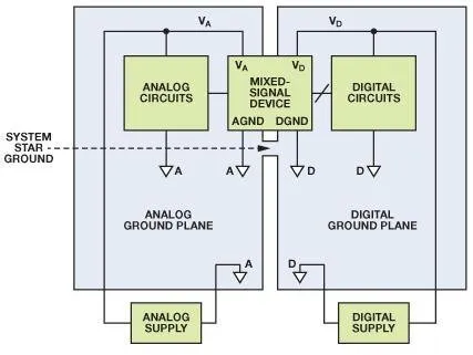
The interaction between ground and power planes influences interplane capacitance, which can filter noise if spaced appropriately. Closer power-ground pairs offer better decoupling, but excessive capacitance strains power delivery networks. Field fringing at plane edges requires stitching vias to maintain shielding effectiveness. These principles guide engineers in optimizing ground plane positions for both low-speed analog and high-speed digital signals.
Best Practices for Ground Plane Layer Stack-Up in Multilayer PCBs
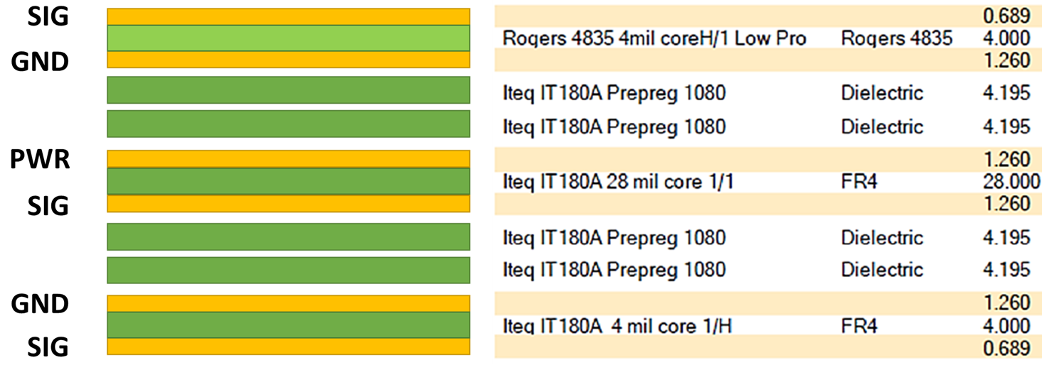
For 2-layer boards, a dedicated ground plane on the bottom layer beneath surface signals provides basic referencing, though limited routing density restricts high-speed use. Engineers route critical traces over solid ground areas, avoiding splits that fragment return paths. This simple ground plane layer stack-up suits low-frequency designs but falls short for impedance control in faster circuits. Vias connect ground pours effectively, minimizing inductance.
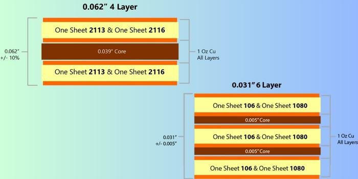
In 4-layer PCB stack-up design, the standard configuration places signal layers on top and bottom, with inner layers as ground and power planes. Top signal over ground, followed by power, then bottom signal creates balanced impedance around 50 ohms for single-ended traces. This setup excels in multilayer PCB design by offering shielding and short return paths. Ground planes should remain solid under high-speed nets, with power planes shaped to avoid overlaps that cause capacitive coupling.
Six-layer and higher configurations expand options for high-speed stack-up, dedicating multiple full ground planes adjacent to signal layers. A common arrangement is signal-ground-signal-power-ground-signal, ensuring every high-speed layer references a plane within 5-10 mils. This impedance control stack-up supports differential pairs with tight tolerances, crucial for USB or PCIe interfaces. Alternate power and ground planes throughout the stack for uniform capacitance distribution.
Optimizing for High-Speed Stack-Up and Impedance Control
High-speed stack-up demands ground planes directly referencing fast edges to suppress resonances and maintain eye diagrams. Place the primary ground plane under the outermost signal layer, using thin prepregs for sub-100 ps rise times. Differential pairs benefit from symmetric ground referencing on both sides, minimizing skew. Simulate stack-up effects early to verify impedance profiles match requirements.
Power plane proximity to ground forms distributed capacitors, but maintain 10-20 mil separation to limit short-circuit risks during lamination. Stitch ground planes with vias every 1/20 wavelength at the highest frequency for RF integrity. In dense designs, dedicate inner layers solely to ground to avoid routing interruptions.
Common Pitfalls in Ground Plane Configuration and Troubleshooting
Splits in ground planes under high-speed traces force return currents to detour, increasing EMI and bit errors. Bridge splits with narrow traces or zero-ohm resistors only if unavoidable, preferring full planes. Asymmetric stack-ups cause warpage, violating flatness specs; balance copper weights across layers.
Voids from fabrication defects degrade shielding; specify minimum annular ring sizes per standards. Over-etching thins planes, raising resistance; control etch factors tightly. Troubleshoot by reviewing stack-up drawings against electrical tests, adjusting prepreg counts for symmetry.
Conclusion
Selecting the right PCB ground plane stack-up configuration integrates electrical performance with manufacturability for reliable designs. Prioritize adjacent planes for signals, symmetry for stability, and continuity for low impedance in multilayer PCB design. High-speed stack-up benefits from dedicated referencing layers, ensuring impedance control and EMI mitigation. Apply these structured principles to tailor configurations for your project's needs. Consult standards like IPC-2221 during planning to align with proven practices.
FAQs
Q1: What is the ideal ground plane layer stack-up for a high-speed stack-up in 4-layer PCBs?
A1: In 4-layer high-speed stack-up, position a full ground plane directly under the top signal layer, followed by a power plane, then the bottom signal layer. This provides low-inductance return paths and controlled impedance around 50 ohms for single-ended signals. Thin dielectrics enhance coupling while maintaining manufacturability. This configuration minimizes crosstalk and supports data rates up to several Gbps effectively.
Q2: How does ground plane placement affect impedance control stack-up?
A2: Ground plane adjacency to signal traces defines the transmission line geometry, directly influencing characteristic impedance. Closer spacing reduces impedance variations but requires precise dielectric control. Multiple ground planes in multilayer setups allow fine-tuning for differential pairs. Engineers verify via TDR measurements post-prototype. Proper placement ensures signal integrity across frequencies.
Q3: Why avoid splits in PCB stack-up design ground planes for multilayer PCB design?
A3: Splits disrupt return current paths, creating large loops that radiate EMI and cause signal reflections. In multilayer PCB design, continuous planes provide the lowest impedance reference. Use stitching vias around splits if necessary for isolated sections. This maintains shielding and complies with performance standards.
Q4: What role do ground planes play in EMI reduction for high-speed stack-up?
A4: Ground planes shield signals and offer low-impedance returns, confining fields between layers. In high-speed stack-up, solid planes adjacent to traces suppress edge radiation. Symmetric configurations further balance fields. Vias tie planes together for uniform potential. This integral approach enhances EMC compliance.
References
[1] IPC-2221 — Generic Standard on Printed Board Design. IPC
[2] IPC-6012E — Qualification and Performance Specification for Rigid Printed Boards. IPC, 2017
[3] IPC-A-600K — Acceptability of Printed Boards. IPC, 2020


