Introduction
In modern high-speed electronics, printed circuit boards (PCBs) must maintain precise signal integrity to support data rates exceeding several gigabits per second. Impedance control testing verifies that transmission lines on the PCB match the designed characteristic impedance, preventing reflections that degrade performance. This process is critical during manufacturing to ensure compliance with design specifications and industry benchmarks. Electrical engineers rely on standardized PCB impedance testing methods to validate multilayer stackups where dielectric variations can alter impedance values. Without proper verification, issues like signal distortion or crosstalk emerge, compromising system reliability. This article explores the principles, methods, and best practices for effective impedance control verification.
What Is PCB Impedance Control Testing and Why It Matters
PCB impedance control testing measures the electrical characteristics of traces to confirm they align with target values specified in the design. Characteristic impedance arises from the interaction between conductor geometry and surrounding dielectric materials, typically targeted at 50 ohms for single-ended lines or 100 ohms differential. Compliance ensures minimal signal reflections, which is vital for applications in telecommunications, computing, and automotive electronics. Deviations beyond tolerance, often ±10%, lead to insertion loss or timing errors in high-frequency signals. Factory-driven insights emphasize testing on production panels using dedicated coupons to represent actual board conditions. Adhering to PCB testing standards guarantees repeatability and traceability across manufacturing lots.
Technical Principles of Impedance in PCBs
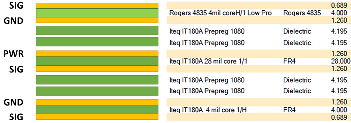
Characteristic impedance in PCBs follows transmission line theory, where Z0 = sqrt(L/C), with L as inductance per unit length and C as capacitance per unit length. Trace width, thickness, dielectric height, and material properties like dielectric constant (Dk) directly influence these parameters. For stripline configurations, the reference planes sandwich the trace, providing stable impedance, while microstrips expose one side to air, increasing sensitivity to manufacturing variations. Engineers calculate initial values using stackup models, but fabrication factors such as plating thickness or etch tolerances introduce discrepancies. Understanding these mechanisms allows precise specification of tolerances during design handover. Variations in glass transition temperature or resin content in laminates further affect Dk, underscoring the need for controlled material selection.
PCB Impedance Testing Methods
Several established PCB impedance testing methods exist, with Time Domain Reflectometry (TDR) being the most common for manufacturing verification. TDR sends a fast-rising step signal along the trace and analyzes reflections from impedance discontinuities, plotting impedance versus position. This method excels in identifying localized variations, such as at vias or etch nonuniformities. Vector Network Analyzer (VNA) testing, operating in the frequency domain, measures S-parameters to derive impedance via calibration standards. VNA suits broader frequency sweeps for insertion loss correlation but requires more setup time. Both methods use edge-launched or soldered SMA connectors on test coupons, ensuring accurate launch conditions.
IPC-TM-650 2.5.5.7 outlines the TDR procedure specifically for characteristic impedance on printed boards, promoting consistent results across facilities.
Impedance Testing Equipment Overview
Impedance testing equipment falls into two categories: time-domain and frequency-domain systems. TDR instruments feature pulse generators with rise times under 50 picoseconds, samplers, and software for impedance extraction using launch point extrapolation to mitigate connector effects. These systems connect via coaxial probes or fixtures, scanning multiple traces sequentially. VNA equipment employs swept sine waves from DC to tens of GHz, with calibration kits including opens, shorts, and loads for de-embedding. Portable TDR units facilitate inline production checks, while benchtop VNAs offer higher resolution for design validation. Selection depends on frequency range and tolerance requirements, with equipment resolution targeting better than ±1 ohm accuracy.
PCB Testing Standards for Impedance Control
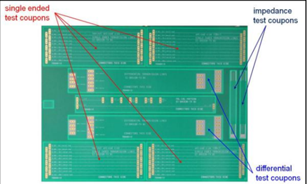
PCB testing standards provide frameworks for impedance control verification, ensuring interoperability in global supply chains. IPC standards define test coupon geometries, such as stripline and microstrip pairs, with specific lengths to minimize end effects. These coupons, etched on production panels, capture stackup realities including core and prepreg variations. Tolerance verification typically averages multiple measurements, rejecting lots if exceeding specified bands. Compliance with such standards mitigates risks in high-reliability sectors like aerospace. Engineers integrate these into qualification flows per IPC-6012 performance specifications.
Best Practices for Impedance Control Verification
Designers specify impedance targets, geometries, and tolerances early, providing stackup drawings with material Dk values. Manufacturers confirm via test coupons positioned away from panel edges to avoid warping influences. Perform TDR scans at multiple points along traces, averaging five readings per line for statistical confidence. Calibrate equipment daily against known standards, and document environmental conditions like temperature and humidity, as they impact dielectric properties. Post-etch testing precedes lamination for multilayer boards, allowing adjustments. Collaborate with fabricators on coupon placement to represent critical nets.
Common Challenges and Troubleshooting in Impedance Testing
Impedance deviations often stem from dielectric thickness variations or etch control issues. If TDR shows step changes, inspect for plating buildup or under-etching using microscopy. Frequency-dependent effects, like skin effect losses, appear as rising impedance tails in plots; correlate with VNA for validation. Connector launch mismatches cause initial spikes, addressed by extrapolation techniques per standards. Panel warpage from asymmetric builds alters clearances, necessitating flat fixturing during tests. Systematic troubleshooting involves cross-referencing design simulations with measurements to refine future stackups.
Case Study: Verifying High-Speed Differential Pairs
Consider a 12-layer PCB for a networking interface targeting 100-ohm differential impedance on inner layers. Initial TDR on coupons revealed +8% deviation due to prepreg thickness scatter. Adjusting press cycles normalized dielectric spacing, with retesting confirming compliance within ±5%. This iterative approach, guided by IPC-TM-650 methods, prevented yield losses. Engineers analyzed via profiles to isolate via stub contributions, optimizing stub lengths. Such factory insights highlight proactive verification's role in meeting PCB compliance testing goals.
Conclusion
PCB impedance control testing remains essential for high-performance electronics, bridging design intent with manufacturing reality. By employing TDR and VNA methods alongside established standards, engineers achieve reliable signal integrity. Best practices like precise coupon design and environmental control minimize variations. Troubleshooting common discrepancies ensures robust compliance. Ultimately, rigorous impedance control verification upholds quality in demanding applications, fostering innovation in electrical engineering.
FAQs
Q1: What are the primary PCB impedance testing methods used in manufacturing?
A1: TDR and VNA represent the core PCB impedance testing methods, with TDR favored for quick production scans and VNA for detailed frequency analysis. TDR detects discontinuities via reflections, while VNA derives impedance from S-parameters. Both require calibrated test coupons on panels. Standards like IPC-TM-650 guide implementation for accuracy.
Q2: How does impedance testing equipment ensure accurate PCB compliance testing?
A2: Impedance testing equipment like TDR systems uses high-speed pulses and extrapolation to measure trace characteristics precisely. VNAs provide swept-frequency data for broadband validation. Daily calibration and proper fixturing maintain resolution under ±1 ohm. This supports PCB compliance testing by verifying design specs across lots.
Q3: What role do PCB testing standards play in impedance control verification?
A3: PCB testing standards such as IPC-TM-650 2.5.5.7 define TDR procedures, coupon designs, and tolerance criteria for impedance control verification. They ensure consistent results despite material or process variations. Compliance demonstrates adherence to industry benchmarks, reducing field failures in high-speed designs.
Q4: Why is impedance control critical for high-speed PCB applications?
A4: Impedance control prevents reflections that cause signal distortion in high-speed PCBs. Verification confirms traces match 50-ohm or differential targets, aligning with design simulations. Factory testing on coupons captures real stackup effects. This upholds performance in data-heavy systems.
References
IPC-TM-650 2.5.5.7 — Characteristic Impedance of Lines on Printed Boards by TDR. IPC.
IPC-2141A — Design Guide for the Control of Electrical Parameters on Printed Board Circuits. IPC, 2003.
IPC-6012E — Qualification and Performance Specification for Rigid Printed Boards. IPC, 2017.


