Introduction
In the realm of PCB design, the layout phase serves as the pivotal bridge between schematic concepts and functional hardware. Engineers must prioritize PCB layout tips that ensure signal integrity, thermal stability, and mechanical reliability to achieve robust designs. Poor layout decisions often lead to issues like crosstalk, overheating, or manufacturing defects that compromise product lifespan. By adhering to established PCB design best practices, designers can mitigate these risks and optimize performance across diverse applications. This article explores essential PCB layout techniques tailored for electric engineers seeking reliable outcomes.
Why PCB Layout Matters for Robust Designs
PCB layout directly influences electrical performance, electromagnetic compatibility, and long-term durability. A well-executed layout minimizes parasitic effects such as inductance and capacitance that degrade high-speed signals. It also facilitates efficient heat dissipation, preventing hotspots that accelerate component failure. In high-density boards, improper placement exacerbates warpage during reflow soldering, leading to assembly failures. Ultimately, robust PCB design hinges on layout strategies that balance functionality with manufacturability and cost-effectiveness.
Fundamental Technical Principles in PCB Layout
Signal integrity forms the cornerstone of effective PCB layout techniques. Engineers must control trace impedance to prevent reflections, especially in high-frequency circuits where mismatches cause data errors. Length matching for differential pairs reduces skew, ensuring timing alignment critical for protocols like USB or PCIe. Ground planes provide return paths that lower noise and EMI, while split planes for analog and digital sections isolate sensitive signals. These principles stem from guidelines in IPC-2221C, which outlines conductor sizing and spacing to maintain electrical integrity.
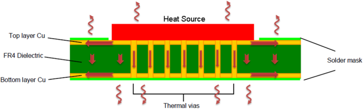
Thermal management requires strategic consideration of heat flow paths. Components with high power dissipation demand vias under thermal pads to conduct heat to inner layers or the opposite side. Copper pours and planes act as heat spreaders, but their thickness and connectivity influence effectiveness. Mechanical stress from CTE mismatches between materials can induce cracks, so symmetric layer stackups minimize warpage. Power distribution networks must avoid voltage drops by using wide traces or planes sized appropriately for current loads.
Essential PCB Design Best Practices for Component Placement
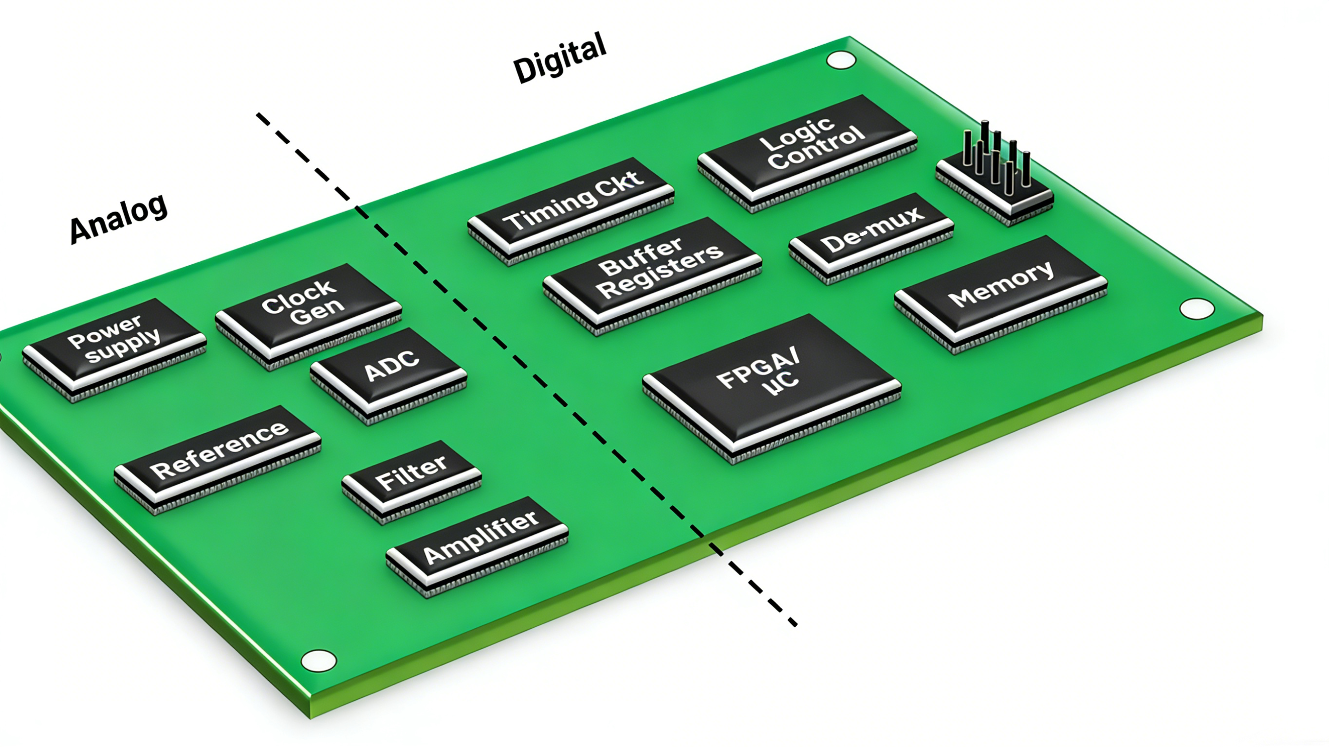
Optimal component placement sets the foundation for PCB layout tips that enhance performance. Group related functions together to shorten traces and reduce loop areas prone to EMI pickup. Separate analog and digital sections with ground barriers to prevent noise coupling into precision circuits. Position high-heat generators near board edges or heatsinks, away from temperature-sensitive ICs like op-amps or sensors. Decoupling capacitors should reside as close as possible to power pins, ideally within 1-2 mm, to suppress transients effectively.
Reserve space for test points and fiducials to aid inspection and alignment during assembly. Consider board handling by placing connectors and mounting holes at edges, avoiding central protrusions that complicate fixturing. For multilayer boards, through-hole components influence inner layer routing, so align them early in the process.
Advanced PCB Layout Techniques for Routing and Layer Management
Routing demands disciplined techniques to uphold PCB design best practices. Prioritize critical nets like clocks and high-speed signals first, using matched lengths and controlled impedance traces. Avoid 90-degree bends, opting for 45-degree or curved corners to minimize reflections and etching undercuts. Differential pairs require tight spacing and parallel routing over uniform reference planes to maintain characteristic impedance.

Layer stackup planning ensures balanced signal and power distribution. Dedicate inner layers to ground and power planes for low-impedance returns and decoupling. Staggered via patterns reduce density while providing redundancy, adhering to annular ring requirements for reliability. IPC-7351B provides land pattern standards that guide pad sizing for optimal solder joints, preventing tombstoning or bridging.
Power Integrity and Grounding Strategies
Power integrity relies on distributed decoupling across the board. Place bulk capacitors near voltage regulators and ceramic caps at every IC power pin. Wide power traces or planes minimize IR drops, calculated based on current density limits. Grounding schemes, such as single-point for low-frequency or multi-point for RF, prevent loops that radiate noise.
Star grounding for analog sections converges returns at a quiet point, while digital grounds tie to a solid plane. Single-point ground connections between planes use beads or resistors to block high-frequency noise. These PCB layout techniques enhance overall system stability.
Thermal and Mechanical Best Practices
Incorporate thermal vias arrays under exposed pads, tented to prevent solder wicking while allowing heat escape. Copper balancing on outer layers reduces warpage, aligning with symmetry rules for multilayer stacks. Mechanical relief slots around mounting holes accommodate expansion differences.
Edge beveling and chamfering ease depaneling stresses. Fixture considerations during layout prevent flexure in automated assembly.
Design for Manufacturability in PCB Layout
DFM integrates seamlessly with PCB design best practices. Maintain minimum clearances between traces, pads, and masks to avoid shorts post-etch. Annular rings around vias ensure plating integrity under drill wander. Panelization rules, like breakaway tabs, facilitate high-volume production without damage.
Silkscreen legends should contrast with solder mask, avoiding overlaps on pads. IPC-2221C emphasizes these spacings to support fabrication tolerances.
Common Pitfalls and Troubleshooting Insights
Engineers often overlook via stitching for plane transitions, leading to impedance discontinuities. Insufficient plane cutouts around vias cause capacitance coupling. Simulate stackups early to verify impedance targets before routing.
Troubleshoot EMI by probing return currents and adding shielding cans where needed. Warpage issues trace to asymmetric copper or poor material selection; iterate with panel-level simulations.
Conclusion
Mastering PCB layout best practices empowers engineers to deliver robust designs that excel in performance and reliability. From precise component placement to meticulous routing and thermal strategies, each technique contributes to minimized risks and optimized outcomes. Integrating standards like IPC-2221C and IPC-7351B ensures compliance and repeatability. Prioritize simulation and review cycles to refine layouts iteratively. Ultimately, thoughtful PCB design elevates products from functional to exceptional.
FAQs
Q1: What are the most important PCB design best practices for high-speed signals?
A1: Focus on controlled impedance traces, length-matched differential pairs, and solid reference planes to minimize reflections and crosstalk. Route critical nets first, avoiding splits in ground planes under them. Use stitching vias along seams and simulate pre-layout for verification. These PCB layout tips ensure signal integrity in demanding applications.
Q2: How do PCB layout techniques improve thermal performance?
A2: Strategic via placement under heat sources channels dissipation to inner planes, while copper pours spread heat evenly. Symmetric stackups prevent warpage, and wide power paths reduce hotspots. Position fans or heatsinks optimally based on airflow simulation. Effective techniques yield cooler, longer-lasting boards.
Q3: Why separate analog and digital sections in PCB design?
A3: Isolation curbs digital noise from corrupting analog precision, vital for ADCs or sensors. Ground planes partitioned with narrow bridges maintain separation without loops. This PCB layout technique boosts dynamic range and reduces spurs in mixed-signal systems.
Q4: What role do standards play in PCB layout tips?
A4: Standards like IPC-2221C define spacings, widths, and patterns for reliability and manufacturability. They guide impedance control and DFM, reducing iterations. Adhering ensures boards meet performance across environments.
References
IPC-2221C — Generic Standard on Printed Board Design. IPC, 2023
IPC-7351B — Generic Requirements for Surface Mount Design and Land Pattern Standard. IPC, 2010
IPC-A-600K — Acceptability of Printed Boards. IPC, 2020


