Introduction
Mixed-signal PCB design combines analog and digital circuits on the same board, creating unique challenges for maintaining signal integrity. Digital signals switch rapidly and generate high-frequency noise, while analog signals require low-noise environments for precision. Poor PCB layout can lead to crosstalk, ground bounce, and electromagnetic interference that degrade performance. Engineers must prioritize signal integrity during layout to ensure reliable operation in applications like data converters and sensors. This article explores key PCB layout techniques to address these issues effectively. By following structured design practices, teams can achieve robust mixed-signal PCB designs.
Understanding Mixed-Signal PCB Design and Signal Integrity
Mixed-signal PCB design integrates analog components, such as amplifiers and filters, with digital logic like microcontrollers and FPGAs. Signal integrity refers to the preservation of electrical signal quality from source to destination, encompassing amplitude, rise time, and timing accuracy. In mixed-signal environments, digital switching induces noise that couples into sensitive analog paths, causing distortion or bit errors. Ground and power distribution networks become critical paths for noise propagation if not managed properly. PCB layout directly influences these interactions through trace routing, layer stacking, and partitioning. Addressing signal integrity early prevents costly respins and ensures compliance with performance specifications.
Engineers evaluate signal integrity risks by analyzing frequency content and coupling mechanisms. High-speed digital signals above 100 MHz demand controlled impedance traces to minimize reflections. Analog sections benefit from shielding to block radiated emissions. Proper layout mitigates these risks systematically. Industry guidelines emphasize separation of noisy and quiet zones to maintain isolation.
Key Principles of Signal Integrity in Mixed-Signal PCBs
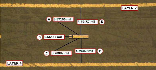
Signal integrity in mixed-signal PCB design hinges on controlled impedance matching to prevent reflections at interfaces. Trace width, spacing, and dielectric thickness determine characteristic impedance, typically 50 ohms for single-ended or 100 ohms for differential pairs. Reflections occur when impedance mismatches cause voltage standing waves, distorting waveforms. Return current paths must remain low-inductance, often via adjacent ground planes. PCB layout engineers calculate these parameters using stackup models for consistency across the board.
Crosstalk arises from capacitive and inductive coupling between adjacent traces, proportional to their proximity and length. In mixed-signal layouts, digital clock lines near analog inputs amplify this effect, injecting noise. Guard traces or stitching vias interrupt coupling fields effectively. Ground bounce from simultaneous switching outputs couples through package inductance into the ground plane. Solid ground planes under signal layers provide equipotential returns, reducing this phenomenon.
Power integrity complements signal integrity by ensuring stable supply voltages. Decoupling capacitors placed close to IC pins shunt high-frequency noise to ground. In mixed-signal designs, separate analog and digital power rails prevent noise sharing. PCB layout positions these elements strategically near loads. Electromagnetic compatibility principles guide shielding to contain emissions.
Per IPC-2221B guidelines, designers select layer counts and materials to support these principles without excessive cost. Thermal expansion matching between layers maintains integrity over temperature cycles.
PCB Layout Techniques for Signal Integrity
Effective PCB layout begins with stackup planning, allocating dedicated planes for analog ground, digital ground, and power. A common four-layer stackup places signals between ground planes for shielding, with power on an inner layer. Splitting grounds requires careful stitching at crossovers to avoid slots in return paths. Mixed-signal PCB design benefits from this isolation, limiting noise migration. Engineers verify stackup symmetry to prevent warpage during fabrication.
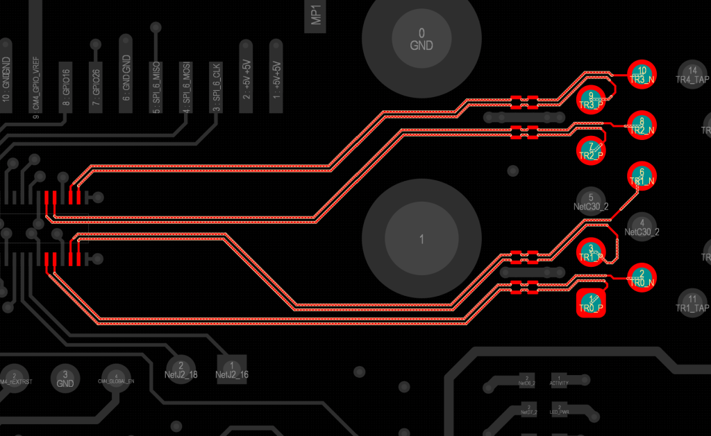
Trace routing follows length-matched paths for differential pairs to preserve common-mode rejection. Avoid right-angle bends, which introduce impedance discontinuities; use 45-degree miters instead. In high-speed sections, route critical signals first on inner layers away from edges. Maintain minimum spacing based on coupling budgets, often 3-5 times trace width. PCB layout tools enforce design rules automatically for consistency.
Via usage demands minimization on high-speed nets due to parasitic inductance. Blind or buried vias reduce stub effects compared to through-hole types. Fanout patterns for BGA packages incorporate short vias with ground vias nearby. For analog traces, route over continuous ground planes to shorten return loops. These techniques enhance signal integrity reliably.
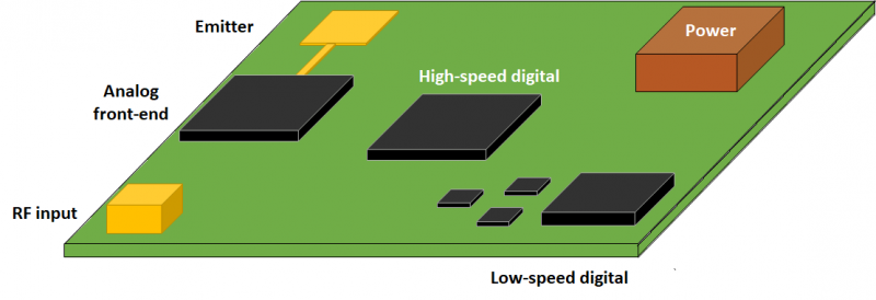
Partitioning divides the board into analog and digital zones, separated by a ground fence of stitched vias. Clocks and high-speed data stay in digital areas, while analog traces avoid crossing partitions. Power entry points use ferrite beads for filtering. Guard rings around sensitive components block stray fields. This zoning is fundamental in mixed-signal PCB design.
Decoupling strategies place capacitors within 1-2 mm of power pins, using multiple values for broadband suppression. Via-in-pad for 0201 capacitors minimizes loop area. Analog supplies receive LC filters for additional isolation. PCB layout verifies clearance for thermal reliefs.
Best Practices and Advanced Design Techniques
Follow a hierarchical routing approach: power and ground first, then high-speed signals, followed by low-speed nets. Use orthogonal routing between layers to reduce coupling. Floorplanning tools help allocate space before routing. In dense boards, backdrilling removes via stubs for signals above 1 GHz. These design techniques optimize signal integrity systematically.
Simulate pre-layout to predict crosstalk and eye diagrams, iterating stackups as needed. Post-layout extraction models parasitics for verification. Mixed-signal PCB design integrates these steps iteratively. Compliance with J-STD-001 ensures assembly processes preserve layout integrity.
For RF-analog integration, microstrip or stripline configurations control radiation. Shield cans over noisy sections contain emissions. Thermal vias under power devices manage heat without distorting planes.
Test points on critical nets facilitate probing without loading effects. Documentation includes fab notes for controlled impedance tolerances, typically ±10%.
Common Challenges and Troubleshooting in Mixed-Signal Layouts
Clock distribution poses risks from skew and jitter coupling into analog PLLs. Length matching within 1 mil tolerances maintains phase alignment. Jitter budgets allocate margins across the chain. Troubleshooting involves TDR measurements to locate discontinuities.
Power plane splits create high-impedance paths if unstitched properly. Splitting capacitors bridge gaps effectively. EMI from board edges requires moats or ground pours. Scope captures during prototyping isolate sources.
Analog distortion from digital return currents demands moat isolation with jumpers. Recheck after EMC testing. These insights guide iterative improvements.
Conclusion
Signal integrity in mixed-signal PCB design relies on meticulous layout planning, from stackup to routing. Partitioning, impedance control, and decoupling form the core techniques. Engineers applying these practices achieve high performance reliably. Adhering to established guidelines minimizes risks across the design cycle. Robust PCB layouts ensure products meet demanding specifications in real-world applications.
FAQs
Q1: What are the main signal integrity challenges in mixed-signal PCB design?
A1: Digital noise coupling into analog circuits via shared grounds or power planes is primary, alongside crosstalk and reflections from impedance mismatches. PCB layout techniques like partitioning and controlled impedance traces mitigate these. Ground bounce from fast switching exacerbates issues. Proper decoupling and shielding resolve most problems logically.
Q2: How does PCB stackup impact signal integrity?
A2: Stackups with adjacent signal-ground planes provide shielding and low-inductance returns, essential for high-frequency signals. Symmetric builds prevent warpage affecting tolerances. Inner power planes distribute current evenly. Mixed-signal designs use split grounds stitched carefully. Verify with field solver tools pre-fabrication.
Q3: What design techniques improve signal integrity in PCB layout?
A3: Length matching for clocks, minimum trace spacing, and guard traces reduce coupling effectively. Orthogonal routing between layers limits broadside crosstalk. Decoupling near pins shunts noise. Backdrilling vias eliminates stubs. These practices ensure clean waveforms in mixed-signal PCB design.
Q4: Why is ground plane partitioning crucial for signal integrity?
A4: It isolates analog quiet zones from digital noise, preventing return current sharing that induces offsets. Stitching vias maintain low-impedance paths across splits. Unpartitioned grounds propagate bounce globally. This technique is standard in PCB layout for precision applications.
References
IPC-2221B — Generic Standard on Printed Board Design. IPC, 2009
IPC-6012D — Qualification and Performance Specification for Rigid Printed Boards. IPC, 2015
J-STD-001H — Requirements for Soldered Electrical and Electronic Assemblies. IPC, 2020


