Introduction
In RF PCB design, routing traces for high-frequency signals presents unique challenges compared to digital or low-frequency circuits. At frequencies above 100 MHz and into the GHz range, signals behave as transmission lines where wavelength dimensions approach trace lengths, leading to effects like reflections and attenuation. Signal loss degrades amplifier efficiency and receiver sensitivity, while noise from crosstalk or electromagnetic interference corrupts data integrity. Effective RF routing techniques focus on impedance matching, controlled propagation environments, and isolation strategies to preserve signal quality. This article explores principles and best practices for minimizing these issues in RF applications, drawing on established engineering approaches. Engineers can achieve reliable performance by understanding conductor geometry, dielectric properties, and layout topologies.
Engineers can achieve reliable performance by understanding conductor geometry, dielectric properties, and layout topologies.
Why RF PCB Routing Matters
RF circuits operate where skin effect confines current to trace surfaces, increasing resistance and signal loss with frequency. Dielectric materials contribute losses through dissipation factor, converting signal energy to heat. Noise sources include mutual inductance between adjacent traces and radiated emissions from unbalanced lines. Poor routing amplifies these, causing bit errors in communications or distortion in radar systems. Impedance mismatches create standing waves, reflecting power back to sources and reducing forward gain. Adhering to disciplined RF PCB design ensures compliance with performance margins in telecommunications, wireless sensors, and microwave modules.
The economic impact underscores the need for precise routing. Rework or redesign due to signal integrity failures escalates costs in production. High-reliability sectors demand routing that meets qualification criteria under thermal and mechanical stress. Ground plane integrity prevents return path inductance, which induces noise voltage drops. By prioritizing RF routing techniques early, designers mitigate risks across the signal chain from antenna to processor.
Fundamentals of Signal Propagation in RF PCBs
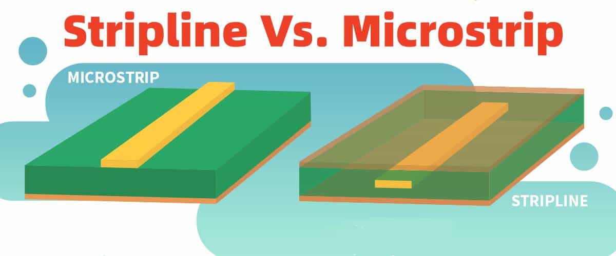
Transmission line theory governs RF signal behavior, treating traces as distributed inductors and capacitors. Characteristic impedance Z0 derives from trace width, thickness, spacing to ground, and substrate properties. Microstrip lines expose one side to air, simplifying fabrication but increasing radiation and sensitivity to nearby components. Stripline configurations sandwich traces between ground planes, offering better shielding at the cost of higher insertion loss from dual dielectrics. Selecting between microstrip and stripline depends on frequency, power levels, and enclosure constraints.
Signal loss mechanisms split into conductor and dielectric components. Conductor loss rises with skin depth reduction, favoring smoother copper surfaces and wider traces within Z0 limits. Dielectric loss scales with dissipation factor tan δ and frequency squared, necessitating low-loss laminates. Noise couples capacitively or inductively between aggressor and victim traces, with coupling coefficient peaking at quarter-wavelength spacing. Return path discontinuities, like split planes, elevate common-mode noise. Maintaining continuous ground references suppresses these effects systematically.
Impedance Matching in RF Routing
Impedance matching prevents reflections quantified by voltage standing wave ratio, ideally near 1:1 for 50-ohm systems. Trace width calculators use formulas incorporating dielectric constant εr, height to ground h, and thickness t. Variations in stackup tolerances alter Z0, demanding process controls during fabrication. T-junctions or unmitigated bends introduce discontinuities exceeding 10% Z0 deviation. Compensating with open stubs or series capacitors restores matching, though parasitics limit broadband efficacy.
In multilayer boards, symmetric stripline achieves tighter Z0 tolerance over microstrip due to enclosed fields. Edge-coupled differential pairs for balanced signals require equal lengths and symmetric gaps to minimize common-mode conversion. Vias pose stubs that resonate at f = c/(4*stub length), necessitating back-drilling or blind vias. Per IPC-2221 guidelines, conductor spacing prevents excessive coupling while allowing dense routing. Simulations verify matching before layout finalization.
Techniques for Minimizing Signal Loss
RF routing techniques prioritize short, straight paths to reduce propagation distance. Serpentine meanders equalize lengths in arrays but introduce extra loss from bends; mitered 45-degree corners preserve Z0 better than sharp 90-degree turns. Via minimization employs direct layer transitions or embedded components, as each via adds 0.5–2 dB loss at GHz frequencies. Surface roughness scatters fields, elevating loss beyond smooth plating models.
Dielectric selection influences loss tangent directly; lower tan δ suits higher bands. Thicker dielectrics lower Z0 for given width, but increase radiation in microstrips. Power handling improves with wider traces, trading off density. Thermal vias under high-power lines dissipate heat, preventing copper migration. Consistent routing width avoids taper losses at transitions.
Strategies for Noise Reduction
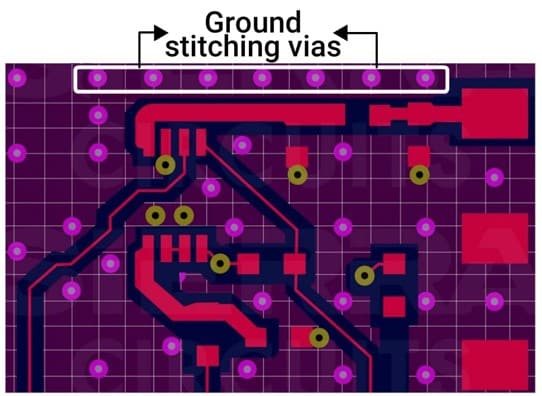
Crosstalk mitigation starts with trace separation exceeding three times dielectric height for capacitive coupling below -30 dB. Guard traces grounded at intervals absorb inductive noise without introducing stubs. Partitioning RF analog from digital sections via ground walls or moats blocks substrate coupling. Stitching vias along plane edges, spaced at λ/20, form Faraday cages around sensitive nets.
Shield cans over RF sections contain emissions, connected with multiple vias for low inductance. Decoupling capacitors near IC pins shunt high-frequency noise to ground. Differential routing rejects common-mode noise inherently, provided symmetry. Environmental factors like enclosure coupling require iterative EMI scans. These layered defenses achieve noise floors below thermal limits.
Layer Stackup and Routing Best Practices
Optimal stackup places RF signals on inner layers for stripline benefits, reserving outer for connectors. Core and prepreg thicknesses dictate h, tuned iteratively for Z0. Power planes adjacent to signals provide low-impedance returns. Routing topology avoids crossing splits; curved paths around obstacles preserve field uniformity.
IPC-6018 specifies performance metrics for high-frequency boards, including attenuation limits. BGA fanouts demand precise via-in-pad for RF outputs. Length tuning compensates group delay variations in phased arrays. Documentation includes stackup drawings and Z0 targets for fabrication alignment.
Component placement groups RF chains linearly, minimizing interconnects. Keep amplifiers close to antennas, routing IF separately. Simulate S-parameters to predict loss and crosstalk pre-prototype.
Troubleshooting Common RF Routing Issues
Excessive loss often traces to via count or roughness; measure TDR for Z0 steps. High noise indicates ground voids; thermal imaging reveals hot spots from poor returns. Reflections show on VNA as S11 peaks; adjust stubs accordingly. Fabrication variances shift Z0 by 5–10%; specify tolerances per IPC-2228 for RF designs.
Iterative prototyping with vector network analyzers validates routing. Common pitfalls include overlooking solder mask effects on microstrip Z0 or via barrel plating thinness. Systematic verification ensures production yield.
Conclusion
Mastering PCB routing for RF applications hinges on balancing impedance matching, loss minimization, and noise isolation through disciplined techniques. Microstrip suits accessible designs, while stripline excels in shielded environments. Ground integrity and via strategies form the backbone of robust performance. By integrating these principles, engineers deliver RF PCBs that meet stringent signal integrity demands. Future trends in 5G and beyond will amplify the need for such precision. Prioritizing RF routing techniques yields reliable, high-performance systems.
FAQs
Q1: What role does impedance matching play in RF PCB design?
A1: Impedance matching ensures maximum power transfer and minimal reflections in RF PCB design by aligning trace Z0 with source and load, typically 50 ohms. Mismatches cause return loss, quantified as VSWR, degrading efficiency. Use field solvers to compute width from stackup parameters. Maintain consistency across transitions to avoid ripples. This foundation supports broadband operation in wireless modules.
Q2: How do microstrip and stripline differ in noise reduction for RF routing?
A2: Microstrip lines radiate more due to open fields, increasing EMI susceptibility, while stripline confines fields between planes for superior noise reduction. Stripline crosstalk drops faster with separation, ideal for dense layouts. Microstrip eases probing but demands wider clearances. Select based on frequency and shielding needs. Both require Z0 control for low noise floors.
Q3: What are key RF routing techniques to minimize signal loss?
A3: RF routing techniques include mitered bends, via minimization, and smooth copper to curb conductor loss. Low tan δ dielectrics tackle dielectric attenuation. Short paths and symmetric pairs preserve integrity. Stitching vias enhance returns, cutting inductive drops. Verify with simulations targeting less than 1 dB per inch loss.
Q4: Why is ground plane design critical for noise reduction in RF PCBs?
A4: Ground planes provide low-impedance returns, suppressing noise from path inductance in RF PCBs. Stitching prevents slots that resonate and couple noise. Separate analog and digital grounds avoid digital switching injection. Continuous planes under traces minimize radiation. This setup achieves isolation exceeding 40 dB.
References
IPC-2221B — Generic Standard on Printed Board Design. IPC, 2009
IPC-6018C — Qualification and Performance Specification for High Frequency (Microwave) Printed Boards. IPC, 2013
IPC-2228 — Sectional Design Standard for High Frequency (RF)/Microwave Printed Boards. IPC, 2018


