Introduction
PCB routing forms the backbone of any printed circuit board design, determining how effectively signals travel between components. Efficient trace layout ensures minimal signal degradation, reduced electromagnetic interference, and reliable performance across various applications. For electric engineers, mastering PCB routing strategies becomes essential when dealing with high-speed signals, dense layouts, and stringent manufacturability requirements. Poor routing can lead to crosstalk, impedance mismatches, and timing issues that compromise overall system functionality. This guide explores key PCB routing techniques, comparing manual versus auto routing approaches, detailing differential pair routing for balanced signals, and emphasizing practices for signal integrity. By understanding these methods, engineers can optimize board performance while adhering to established design principles.
Routing decisions impact not just electrical characteristics but also thermal management and mechanical reliability. In multilayer boards, trace placement influences layer stackup efficiency and via usage. Engineers must balance routing density with clearance rules to avoid shorts or opens during fabrication. Advances in high-frequency applications demand precise control over trace geometry and length. This comprehensive overview provides logical steps to implement robust PCB routing strategies tailored for complex designs.
What Is PCB Routing and Why It Matters
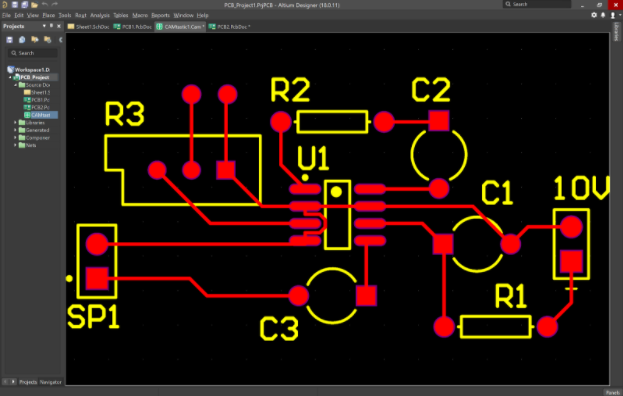
PCB routing refers to the process of defining conductive paths, or traces, that interconnect components on a printed circuit board. These traces carry electrical signals, power, and ground, forming the electrical network of the board. Routing begins after component placement and schematic capture, transforming a netlist into physical pathways. Engineers consider factors like trace width, spacing, length, and vias to meet electrical, thermal, and manufacturing constraints. Effective routing minimizes signal loss, prevents noise coupling, and supports high-speed data transmission.
The importance of PCB routing lies in its direct influence on signal integrity and board reliability. In high-speed designs, improper routing introduces reflections, attenuation, and crosstalk, leading to bit errors or system failures. For power distribution, wide traces reduce voltage drops and heat generation. Routing also affects electromagnetic compatibility by controlling loop areas and return paths. Adhering to guidelines in IPC-2221 ensures consistent conductor spacing and layout solvability, promoting designs that perform reliably in real-world conditions. Ultimately, skilled routing enables compact, cost-effective boards without sacrificing functionality.
Manufacturability plays a critical role, as tight routing demands precise fabrication tolerances. Overly dense traces increase the risk of defects like shorts or etchant undercuts. Engineers evaluate routing completeness early to identify fanout issues or congestion hotspots. By prioritizing critical nets, they allocate resources efficiently across layers. This structured approach aligns design intent with production capabilities, reducing iterations and time-to-market.
Core PCB Routing Strategies
PCB routing strategies encompass a range of techniques to achieve optimal trace layout while addressing design constraints. Engineers start by classifying nets into categories such as high-speed signals, power, and analog lines, each requiring specific handling. Critical signals receive priority routing to secure preferred paths before filling remaining space. Layer assignment follows stackup planning, placing fast signals on inner layers adjacent to reference planes for better impedance control. Vias serve as interlayer connections, but their placement requires minimization to preserve signal quality.
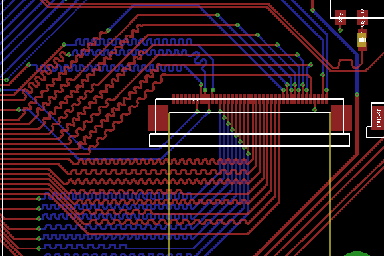
One fundamental strategy involves orthogonal routing, where traces run horizontally on one layer and vertically on another to reduce coupling. Curved traces over straight lines reduce reflections at bends, especially for high frequencies. Teardrops at via-trace junctions prevent drill breakout and improve adhesion. Engineers also employ length tuning, such as serpentine patterns, to match propagation delays across parallel signals. These methods collectively enhance PCB routing strategies for dense, high-performance boards.
Flooding ground or power planes provides low-impedance returns and shielding. However, splits in planes demand careful bridging to avoid interrupting current paths. Simulation tools verify strategies pre-layout, predicting issues like crosstalk before physical prototyping. By integrating these elements, engineers create robust interconnects that support evolving electronic demands.
Manual vs Auto Routing PCB: A Detailed Comparison
Manual routing PCB offers engineers complete control over trace paths, ideal for complex high-speed designs. Designers manually draw traces, adjusting width, spacing, and bends in real-time to meet constraints. This approach excels in differential pair routing PCB and impedance-sensitive nets, where auto routers often fall short. Manual methods allow precise length matching and avoidance of noisy areas. However, it demands significant time and expertise, especially on dense boards with thousands of nets.
Auto routing PCB, conversely, uses algorithms to generate traces based on predefined rules like spacing and via costs. It accelerates layout for simple or medium-complexity boards, routing power and ground nets efficiently. Modern auto routers incorporate rip-up and retry functions to optimize paths iteratively. Yet, they struggle with high-speed signals, producing suboptimal routes that violate signal integrity rules. Engineers often use auto routing as a starting point, then manually refine critical sections.
The choice between manual versus auto routing PCB depends on project specifics. For low-speed consumer boards, auto routing suffices, saving design cycles. High-reliability applications, like aerospace or telecom, favor manual routing for verified performance. Hybrid workflows combine both: auto route non-critical nets, manual handle differentials and clocks. This balances speed and precision, ensuring manufacturable layouts. Post-routing, design rule checks (DRC) validate compliance regardless of method.
In practice, manual routing fosters deeper understanding of signal behavior, aiding troubleshooting. Auto routing risks "black box" outputs hard to debug. Training emphasizes manual skills first, then algorithmic leverage. Ultimately, experienced engineers blend techniques for efficient outcomes.
Differential Pair Routing PCB Techniques
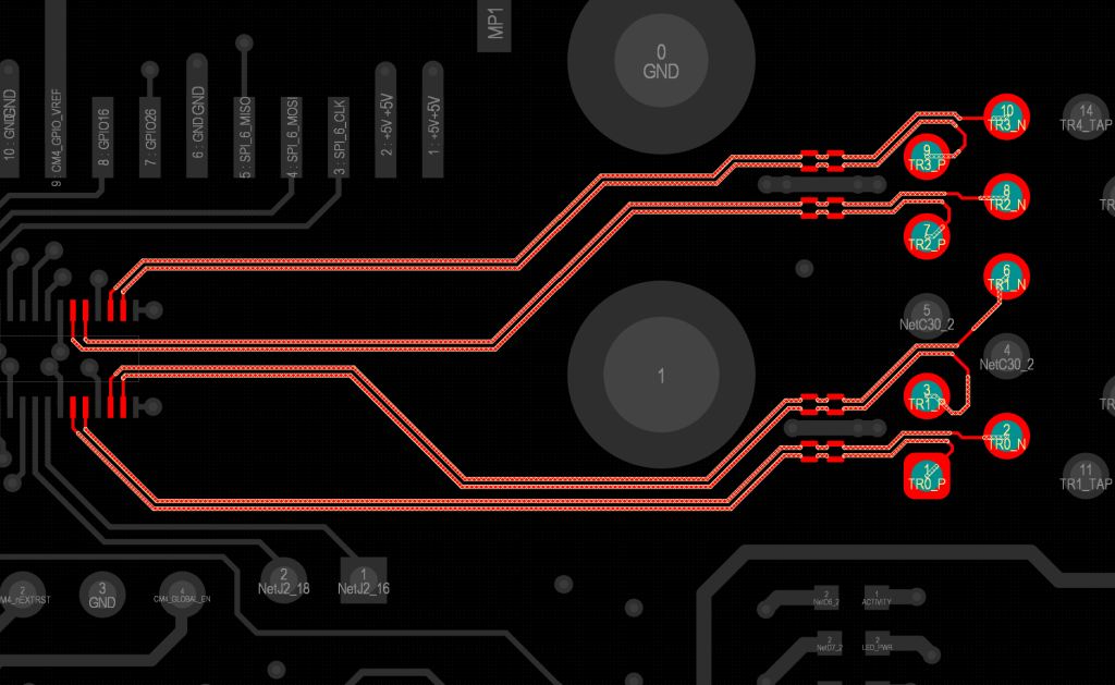
Differential pair routing PCB transmits balanced signals using two closely spaced traces carrying equal but opposite voltages. This configuration rejects common-mode noise, crucial for USB, PCIe, and LVDS interfaces. Key techniques include maintaining constant spacing and equal lengths to preserve differential impedance and skew. Traces route parallel without sharp bends or vias unless matched on both lines. Intra-pair spacing typically follows edge-coupled microstrip or stripline geometries.
Length matching ensures signals arrive simultaneously, minimizing timing skew. Serpentine or trombone patterns adjust longer traces without altering impedance. Vias in differential pairs require stitching grounds nearby for return path integrity. Engineers calculate pair width and gap using stackup parameters, targeting 85-120 ohms differential impedance. IPC-2141A provides guidelines for high-speed controlled impedance, aiding precise geometry selection.
Routing avoids crossing other signals or splitting planes to prevent mode conversion. Preferred paths lie over solid reference planes, with 3:1 spacing to adjacent traces reducing crosstalk. Fanout from connectors demands fanning out pairs symmetrically. Post-layout verification measures skew below 10 ps typically. These practices ensure reliable data transmission up to multi-Gbps rates.
Advanced multilayer boards dedicate pairs to inner layers for shielding. Blind or buried vias minimize stub effects. Simulation confirms eye diagrams pre-fabrication. By following these steps, differential pair routing PCB upholds signal integrity in demanding environments.
PCB Routing for Signal Integrity
PCB routing for signal integrity focuses on preserving waveform quality from driver to receiver. Key challenges include impedance discontinuities, crosstalk, and ground bounce. Controlled impedance traces match source and load to prevent reflections, calculated per layer stackup. IPC-2221 outlines conductor sizing and spacing to mitigate interference. Reference planes adjacent to signal layers provide low-inductance returns, essential for GHz signals.
Crosstalk minimization demands adequate spacing: forward and backward coupling decrease with distance. Orthogonal routing between layers further reduces coupling. Avoid stubs by using back-drilling or blind vias for high-speed lines. Trace bends employ 45-degree angles or smooth curves to limit return loss. Power planes decouple noise through bypass capacitors placed strategically.
Via optimization counts transitions, favoring fewer wider vias for low inductance. Length-matched groups like clocks and data buses prevent skew-induced errors. Thermal vias under power traces aid heat dissipation without signal impact. Pre-layout planning allocates escape routes for BGA packages. Hyperlynx or similar simulations predict SI metrics like insertion loss.
Ground plane partitioning isolates analog and digital sections, with stitching vias bridging splits. Decoupling strategies integrate with routing flow. Compliance with IPC-6012E ensures fabricated boards meet performance specs. These holistic measures deliver clean signals in noisy environments.
Best Practices for Implementation
Implement PCB routing best practices by establishing a hierarchical net priority list. Route clocks and differentials first, followed by other high-speed signals, then power and singles. Maintain minimum clearances per voltage levels, scaling with board thickness. Use grid-based routing for alignment, snapping to 0.1 mil increments where precision matters.
Layer utilization maximizes inner layers for signals, outer for components. Plane clearance around vias prevents shorts. Annotate routes with net names for review. Iterative DRC runs catch violations early. Document routing decisions in reports for team handover.
For high-density interconnects, microvias enable tighter pitches. Test coupons validate impedance post-fab. Collaborate with fabricators on DFM rules. These practices streamline workflows and elevate design quality.
Conclusion
Mastering PCB routing techniques unlocks efficient trace layouts that drive superior board performance. From manual versus auto routing choices to specialized differential pair and signal integrity methods, each strategy contributes to reliable designs. Engineers benefit from structured approaches grounded in industry principles like IPC standards. Prioritizing critical nets, controlling impedance, and minimizing discontinuities form the core of effective practices. Apply these insights to reduce risks, enhance manufacturability, and accelerate development cycles.
FAQs
Q1: What are the main PCB routing strategies for high-density boards?
A1: PCB routing strategies for high-density boards emphasize net prioritization, orthogonal layer directions, and microvia usage to maximize space. Engineers route critical high-speed nets manually first, then auto-fill others, ensuring constant impedance and minimal vias. Reference planes shield signals, while length tuning addresses skew. This logical sequence aligns with IPC-2221 guidelines for layout solvability, yielding compact, performant designs. Adhering to these reduces congestion and supports complex topologies.
Q2: How does manual vs auto routing PCB impact signal integrity?
A2: Manual routing PCB provides precise control for signal integrity, allowing custom paths that avoid crosstalk and match lengths accurately. Auto routing excels in speed for low-speed nets but may produce suboptimal routes with impedance variations. Hybrid use combines strengths: manual for differentials, auto for power. Verification via simulation ensures quality. For electric engineers, manual oversight prevents common auto pitfalls like excessive vias.
Q3: Why is differential pair routing PCB critical for high-speed signals?
A3: Differential pair routing PCB rejects noise through balanced transmission, maintaining integrity at high data rates. Equal lengths and spacings preserve impedance, per IPC-2141A principles. Avoid plane splits and use reference planes underneath. This technique minimizes skew and EMI, essential for interfaces like Ethernet. Proper implementation supports multi-Gbps without errors.
Q4: What role does PCB routing for signal integrity play in EMI reduction?
A4: PCB routing for signal integrity reduces EMI by controlling loop areas, ensuring tight coupling to ground planes, and spacing traces adequately. Orthogonal routing and smooth bends limit radiation. Stitching vias bridge plane splits, providing return paths. These practices comply with design standards, lowering emissions and improving compliance.
References
IPC-2221 — Generic Standard on Printed Board Design. IPC
IPC-2141A — Design Guide for High-Speed Controlled Impedance Circuit Boards. IPC
IPC-6012E — Qualification and Performance Specification for Rigid Printed Boards. IPC, 2017


