Introduction
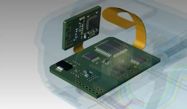
Flex PCBs and rigid-flex circuits have revolutionized electronics by allowing circuits to bend, fold, and conform to irregular shapes in compact devices. These technologies find essential use in wearables, medical implants, aerospace systems, and automotive sensors where traditional rigid boards fall short. However, schematic design for flex and rigid-flex PCBs introduces unique challenges beyond standard rigid board practices. Engineers must anticipate mechanical stresses like PCB bending from the earliest electrical design stages to ensure reliability and manufacturability. This article delves into these challenges, drawing on established engineering principles, and outlines practical solutions for effective flexible circuit design. By addressing schematic-level decisions early, designers can mitigate risks that surface later in layout and fabrication.
Understanding Schematic Design in Flex and Rigid-Flex Contexts
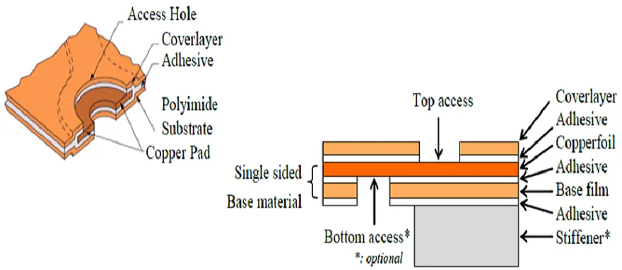
Schematic design traditionally focuses on electrical connectivity, component selection, and signal flow, but flex PCB design requires embedding mechanical awareness into this phase. Flex circuits, made from materials like polyimide, must withstand repeated bending without trace fractures or delamination. Rigid-flex PCBs combine rigid FR-4 sections for components with flexible interconnects, complicating net assignments across varying stackups. Why does this matter? Poor schematic planning leads to layout impossibilities, such as critical signals routed through high-strain bend zones, increasing failure rates in dynamic applications. For electric engineers, mastering schematic design for flex means treating the board as a mechatronic system from the start.
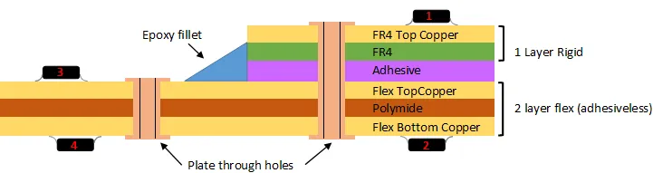
In rigid-flex PCB design, schematics often use hierarchical sheets to represent rigid islands and flex tails separately. This structure aids in managing layer transitions and via restrictions in flex areas. Engineers must define net classes early, flagging traces destined for flex regions to enforce wider widths or special routing rules downstream. Ignoring these steps results in redesign iterations, delaying projects. Standards like IPC-2223E provide foundational guidelines for such sectional designs, emphasizing compatibility between electrical and mechanical domains.
Key Challenges in Schematic Design for Flex Circuits
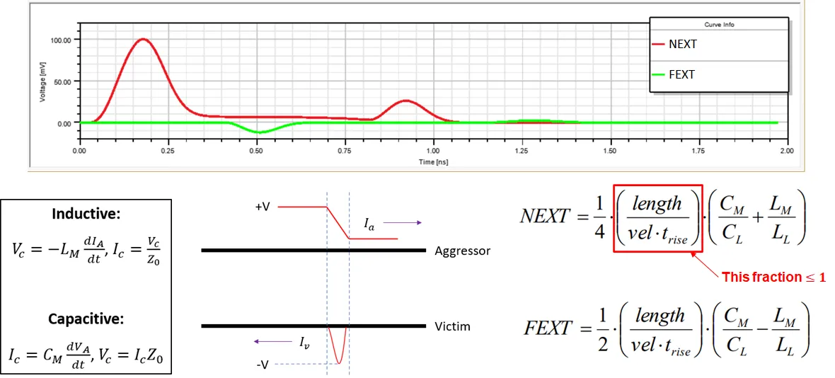
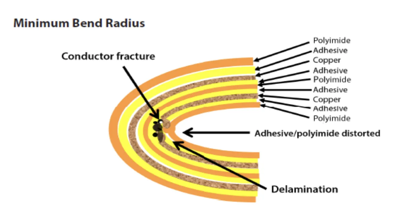
Navigating the schematic phase is a critical first step in any comprehensive guide to flex and rigid-flex design and manufacturing. One primary challenge in schematic design for flex is anticipating strain distribution during PCB bending. Traces in flex zones experience tensile and compressive forces, potentially cracking conductors if paths are not planned for curved routing. Engineers must identify high-flex areas early, assigning signals with lower bend radii to rigid sections.Power and ground nets spanning flex-rigid boundaries risk impedance discontinuities, affecting signal integrity in high-speed designs. Without schematic annotations for bend lines, layout teams struggle to align electrical nets with mechanical outlines.
Component placement constraints pose another hurdle in flexible circuit design. Active devices like ICs cannot reside in flex tails due to solder joint fatigue from movement. Schematics need flags or attributes to restrict certain footprints to rigid zones, preventing downstream errors. Vias and blind vias in transition areas add complexity, as flex layers limit plating options. Thermal management complicates matters, with flex materials having lower thermal conductivity than rigid laminates, requiring distributed dissipation planning at the schematic level.
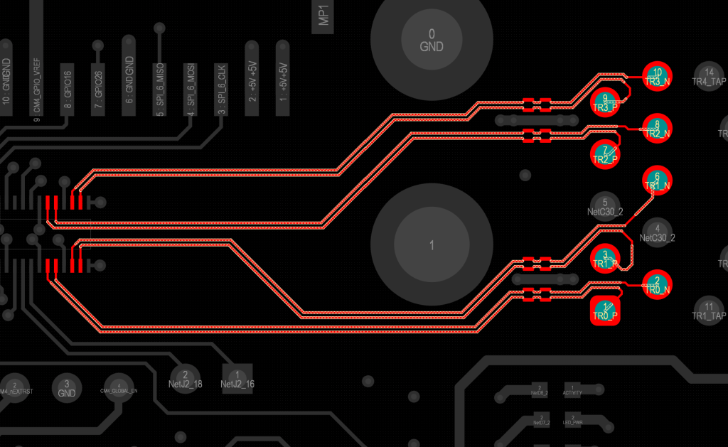
Signal integrity challenges intensify in rigid-flex PCB design. Differential pairs crossing flex regions face varying dielectric constants, altering characteristic impedance. Schematic simulations must model these variations using parameterized models for flex sections. EMI susceptibility rises in folded configurations, necessitating shielded net definitions early. These issues demand a shift from pure electrical thinking to holistic system-level schematics.
Related Reading: Constraint Management Techniques for Flexible and Rigid Flex PCBs
Mechanical-Electrical Integration Principles
The core principle guiding schematic design for flex revolves around defining flex-rigid boundaries upfront. Engineers sketch outline zones in schematic documentation, correlating nets to mechanical features like bend axes. This pre-layout zoning prevents electrical paths from violating minimum bend radii outlined in IPC-6013E. Conductor sizing must account for dynamic stresses, with wider traces in flex areas to reduce resistance changes under flexure. Material interactions, such as adhesive flow during lamination, influence via reliability, so schematics specify stackup-aware net routing.
Impedance control requires schematic-level stackup definitions. Flex dielectrics like coverlay introduce variables absent in rigid designs, so engineers use field solver inputs derived from schematic net classes. Power integrity benefits from dedicated flex ground planes, planned as sheet symbols in hierarchical schematics. Testing provisions, such as test points outside bend zones, integrate seamlessly when schematics include mechanical overlays. These principles ensure the design transitions smoothly to layout.
Best Practices for Overcoming Schematic Challenges
Start with a mechanical outline imported into the schematic environment to visualize flex regions. Assign region-specific net classes: "Flex-Critical" for low-strain signals, "Bend-Tolerant" for power lines. Use hierarchical blocks for rigid-flex sections, linking them with inter-sheet connectors that flag transition constraints. This approach streamlines reviews and automates rule checks. Simulate signal paths across boundaries using flex-aware models to predict discontinuities.
Leverage annotation tools to mark bend allowances and no-component zones. For rigid-flex PCB design, define overlay layers in schematics for coverlay and stiffener placement. Prioritize analog signals in rigid areas to minimize noise pickup during flexing. Collaborate with fabrication early by exporting schematic-derived stackups for DFM feedback. These practices align electrical intent with mechanical reality, reducing iterations.
Incorporate redundancy for critical nets in high-flex applications, duplicating paths across multiple flex layers. Document bend cycle expectations in schematic notes, guiding qualification per IPC-6013E. Opt for surface-mount passives in rigid sections to avoid through-hole stresses at transitions. Regular DRC runs with custom flex rules catch issues pre-layout. By embedding these best practices, engineers achieve robust flexible circuit design.
Suggested Reading: Signal Integrity: PCB Considerations During the Circuit Design
Troubleshooting Common Issues in Flex Schematic Designs
Engineers often encounter netlist mismatches when flex tails connect multiple rigid boards. Solution: Use bus structures in schematics to represent parallel flex runs, ensuring pin swaps align with mechanical folding. Impedance mismatches at transitions manifest as crosstalk; mitigate by grouping pairs in dedicated flex channels from schematic assignment. Component obsolescence in rigid areas disrupts redesigns, so maintain variant schematics with flex-compatible alternatives.
Delamination risks from thermal expansion arise if power planes overload flex adhesives. Balance loads across layers via schematic power tree analysis. High-frequency signals degrading in bends require low-loss dielectrics specified in stackup notes. Prototype schematics with simplified flex models validate assumptions before full layout. These troubleshooting steps preserve design integrity.
Conclusion
Schematic design for flex and rigid-flex circuits demands foresight into mechanical behaviors like PCB bending and strain. By integrating zoning, net classes, and hierarchical structures early, engineers overcome challenges in conductor integrity, signal performance, and manufacturability. Adhering to principles from IPC-2223E and IPC-6013E ensures compliance and reliability. These strategies enable innovative flexible circuit design for demanding applications. Ultimately, a mechanically informed schematic paves the way for efficient layout, fabrication, and long-term performance.
FAQs
Q1: What are the main differences in schematic design for flex versus rigid PCBs?
A1: In flex PCB design, schematics must incorporate mechanical zones for bends, net classes for strain-sensitive traces, and hierarchical sheets for rigid-flex transitions. Rigid designs focus solely on electrical connectivity, ignoring dynamic stresses. This early integration prevents layout conflicts and ensures traces avoid high-strain areas while aligning with standards like IPC-2223E.
Q2: How does PCB bending impact signal integrity in rigid-flex PCB design?
A2: PCB bending alters dielectric spacing in flex sections, causing impedance variations and potential crosstalk. Schematics address this by assigning controlled-impedance net classes and simulating transitions. Avoid routing high-speed signals through bends by designating rigid zones early. Strain relief features, planned at the schematic stage, help maintain performance over bend cycles.
Q3: What best practices improve schematic design for flex circuits?
A3: Define flex-rigid boundaries and bend lines in schematic annotations to guide layout. Use region-specific net classes to enforce wider traces in flex areas. Employ hierarchical designs to manage multi-section rigid-flex systems. Run simulations with flex-aware models to predict discontinuities and verify impedance control before layout.
Q4: Why reference standards like IPC-6013E in flex PCB design schematics?
A4: IPC-6013E outlines qualification and performance criteria for flexible and rigid-flex boards, informing schematic decisions on vias, plating, stackups, and bend durability. Referencing it early ensures compliance with performance classes for dynamic use and reduces costly redesigns later in the process.
References
IPC-2223E — Sectional Design Standard for Flexible/Rigid-Flexible Printed Boards. IPC, 2020
IPC-6013E — Qualification and Performance Specification for Flexible/Rigid-Flexible Printed Boards. IPC, 2021