Introduction
In the realm of printed circuit board design, achieving compatibility between trace width and footprint pad dimensions is a critical factor for ensuring functionality and reliability. Trace width directly influences impedance and current capacity, while footprint pads must align with component specifications for proper soldering and electrical performance. For electrical engineers, understanding these elements is essential to prevent signal integrity issues, thermal problems, and manufacturing defects. This article explores the intricate relationship between trace width and footprint pads, delving into their technical principles, industry standards, and best practices. By addressing impedance control and current capacity, alongside pad design considerations, this content aims to provide actionable insights for optimizing PCB layouts. Whether designing high speed circuits or power heavy applications, mastering these aspects ensures robust and efficient designs.

What Is Trace Width and Footprint Compatibility and Why It Matters
Trace width refers to the physical width of conductive paths on a PCB, determining how much current a trace can carry and affecting its impedance in high frequency applications. Footprint pads, on the other hand, are the designated areas where components are soldered, and their dimensions must match both the component leads and the connecting traces for seamless integration. Compatibility between these two elements ensures that electrical signals transfer without loss, heat dissipation remains manageable, and mechanical stability is maintained during assembly.
The importance of this compatibility cannot be overstated. Mismatched trace widths and pads can lead to increased resistance, signal degradation, or insufficient current handling, risking board failure. For high speed designs, impedance mismatches can cause reflections, while in power circuits, inadequate trace width may result in overheating. Properly aligned designs also ease manufacturing processes, reducing the likelihood of soldering defects. For electrical engineers, prioritizing this balance is fundamental to achieving reliable and efficient PCB performance.
Related Reading: How to Calculate PCB Trace Width for 20A Circuits
Technical Principles of Trace Width and Impedance
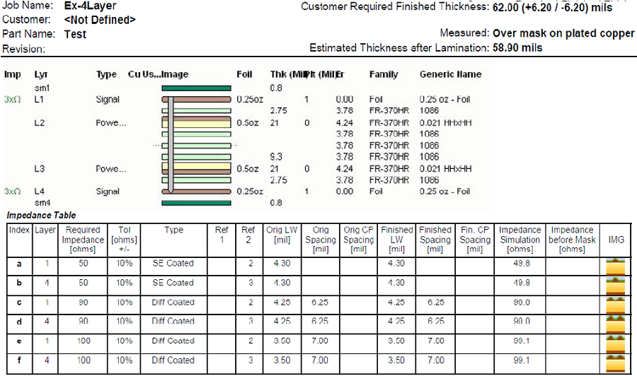
Trace width plays a pivotal role in controlling impedance, a critical parameter in high speed digital and RF circuits. Impedance, measured in ohms, depends on trace width, thickness, dielectric material, and proximity to ground planes. Narrower traces typically result in higher impedance, while wider traces lower it. Maintaining a specific impedance, often 50 ohms for RF signals, requires precise trace width calculations based on the PCB stackup and material properties.
Industry standards provide guidelines for determining appropriate trace widths to achieve desired impedance. These standards outline formulas and charts that account for variables like dielectric constant and trace spacing. Engineers must also consider the skin effect in high frequency applications, where current flows near the surface of the conductor, necessitating careful width selection to minimize losses. Accurate impedance control prevents signal reflections, ensuring data integrity across the circuit.
Current capacity is another crucial aspect influenced by trace width. Wider traces can handle higher currents without excessive heating, as they offer lower resistance. Standards such as IPC-2221B provide detailed charts linking trace width, thickness, and temperature rise to current carrying capacity. For instance, a trace on a standard 1 oz copper layer requires specific widths to safely carry currents without exceeding acceptable temperature limits. Balancing impedance and current needs often requires iterative design adjustments.
Related Reading: How Does PCB Trace Width Affect Impedance?
Footprint Pad Design and Its Relation to Trace Width
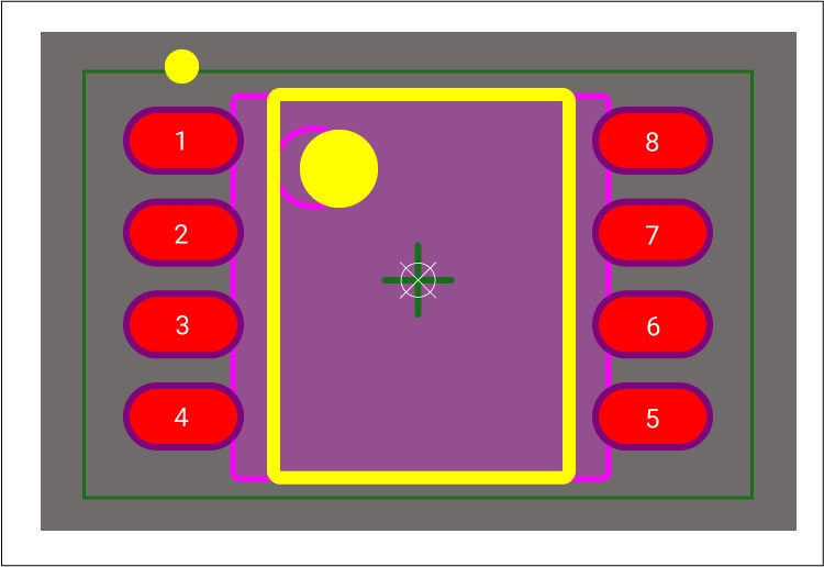
Footprint pads must be designed to accommodate both the component's physical dimensions and the connecting trace width for optimal electrical and mechanical performance. Pad size and shape directly affect soldering quality, thermal dissipation, and signal integrity. If a trace is significantly wider or narrower than the pad it connects to, it can create uneven current distribution or stress points, leading to potential failures.
Industry standards, such as IPC-7351B, offer detailed specifications for surface mount pad dimensions, ensuring compatibility with various component packages. These guidelines define pad sizes based on component lead geometry and tolerance levels, categorized into density levels for different manufacturing capabilities. For through hole components, standards like IPC-2222A provide recommendations on pad diameters relative to hole sizes, ensuring proper trace connections.
When a trace approaches a pad, its width may need adjustment to match the pad's contact area. Sudden changes in width can alter impedance, especially in high frequency designs, causing signal issues. Gradual tapering or necking down of traces near pads helps maintain consistent impedance. Engineers must also consider the pad's thermal relief patterns in power circuits to prevent soldering issues due to excessive heat sinking.
Practical Solutions for Ensuring Compatibility
Achieving compatibility between trace width and footprint pads requires a systematic approach during the design phase. Start by referencing industry standards to select appropriate trace widths based on current capacity and impedance requirements. Use calculators and simulation tools aligned with guidelines from standards like IPC-2221B to determine precise dimensions for your specific application.
For footprint pads, adhere to specifications outlined in IPC-7351B, which categorize land patterns into different density levels based on manufacturing constraints. Select the appropriate level based on your production capabilities to ensure manufacturability. Verify component datasheets for exact pin dimensions and tolerances, then cross reference with standard recommendations to finalize pad sizes.
To address impedance concerns at trace to pad transitions, implement gradual width changes rather than abrupt shifts. This technique minimizes signal reflections in high speed designs. Additionally, ensure that trace routing to pads avoids sharp angles, as these can introduce unwanted inductance or capacitance. For power traces, incorporate thermal reliefs around pads to balance heat distribution during soldering.
Regularly simulate your design to check for potential mismatches. Tools adhering to industry standards can highlight areas where trace width or pad dimensions deviate from optimal values. Adjust your layout iteratively, considering both electrical performance and manufacturing feasibility. Collaboration with fabrication teams early in the design process helps identify constraints that might affect compatibility.
Troubleshooting Common Issues in Trace Width and Pad Compatibility
Mismatches between trace width and footprint pads often manifest as signal integrity problems, overheating, or soldering defects. In high speed circuits, impedance discontinuities at trace to pad junctions can cause signal reflections, leading to data errors. To resolve this, review the trace width transition and adjust for a smoother taper, using simulation to confirm impedance stability.
Overheating in power circuits typically indicates insufficient trace width for the current load. Refer to IPC-2221B charts to recalculate the required width based on copper thickness and acceptable temperature rise. If space constraints prevent widening traces, consider increasing copper weight or adding parallel traces to distribute current.
Soldering issues, such as insufficient wetting or tombstoning, often stem from improper pad dimensions relative to component leads. Cross check pad sizes against IPC-7351B guidelines and component specifications. Adjust pad shapes or add solder mask defined pads if necessary to improve manufacturing yield. Inspecting prototypes under magnification can reveal subtle mismatches for correction in subsequent revisions.
Conclusion
Ensuring compatibility between PCB trace width and footprint pads is a cornerstone of effective design for electrical engineers. Trace width governs impedance and current capacity, while footprint pads secure component connections, making their alignment vital for performance and reliability. By adhering to industry standards like IPC-2221B and IPC-7351B, engineers can achieve balanced designs that meet electrical and manufacturing requirements. Practical solutions, such as gradual trace tapering and thermal relief implementation, address common challenges, while troubleshooting techniques resolve issues like signal reflections and soldering defects. Mastery of these principles enables the creation of robust PCB layouts suited for diverse applications, from high speed to high power circuits.
FAQs
Q1: How does trace width impact current capacity in PCB design?
A1: Trace width directly affects the amount of current a PCB trace can carry without overheating. Wider traces offer lower resistance, allowing higher current capacity. Standards like IPC-2221B provide detailed charts to calculate appropriate widths based on copper thickness and temperature rise limits. Electrical engineers must balance space constraints with these requirements to ensure safe operation.
Q2: Why is impedance control important for trace width in high speed designs?
A2: Impedance control is crucial in high speed designs to prevent signal reflections and ensure data integrity. Trace width, along with dielectric properties and stackup, determines impedance. Matching it to system requirements, often 50 ohms, minimizes losses. Guidelines from standards help engineers select widths for consistent signal performance across the circuit.
Q3: How do footprint pad dimensions affect soldering quality?
A3: Footprint pad dimensions must match component leads for proper soldering. If pads are too small or large, issues like insufficient wetting or tombstoning occur. Standards such as IPC-7351B specify optimal pad sizes and shapes based on component packages. Correct dimensions ensure reliable mechanical and electrical connections during assembly.
Q4: What steps can ensure trace width and footprint pad compatibility?
A4: To ensure compatibility, start by following standards like IPC-2221B for trace width and IPC-7351B for pad design. Use simulation tools to verify impedance and current capacity. Implement gradual width transitions near pads and confirm component specifications. Early collaboration with fabrication teams also helps align designs with manufacturing capabilities.
References
IPC-2221B — Generic Standard on Printed Board Design. IPC, 2012.
IPC-7351B — Generic Requirements for Surface Mount Design and Land Pattern Standard. IPC, 2010.
IPC-2222A — Sectional Design Standard for Rigid Organic Printed Boards. IPC, 2010.
