Introduction
Power integrity in PCB design ensures that components receive clean, stable voltage throughout their operation. Voltage drop along power traces can degrade signal quality, cause timing errors, and lead to system failures in high-performance electronics. Engineers must optimize trace resistance, trace width, and copper weight to maintain low current density and reliable power delivery. This article explores the principles behind power integrity, focusing on minimizing voltage drop through structured design practices. By addressing these elements, designers can enhance overall board reliability and performance.
What Is Power Integrity and Why It Matters
Power integrity refers to the ability of a PCB's power distribution network to deliver stable voltage and current to all loads without excessive noise or droop. In modern electronics with high-speed digital circuits and dense component placement, poor power integrity manifests as voltage drop, ground bounce, and electromagnetic interference. These issues directly impact signal integrity, as fluctuating power rails alter logic thresholds and switching speeds. For electric engineers, maintaining power integrity is critical in applications like processors, FPGAs, and RF modules where even millivolts of deviation can cause malfunction. Industry standards emphasize these considerations to prevent field failures and ensure compliance during qualification testing.
Understanding Voltage Drop and Trace Resistance
Voltage drop occurs due to the inherent resistance in PCB traces, governed by Ohm's law where V = I × R. Trace resistance depends on the material resistivity, primarily copper, trace length, and cross-sectional area determined by trace width and thickness. Longer traces or higher currents exacerbate voltage drop, leading to insufficient voltage at load points and potential brownouts. Current density, defined as current per unit cross-sectional area, must stay below limits to avoid excessive heating and electromigration. Engineers calculate these parameters early to predict and mitigate drops before prototyping.
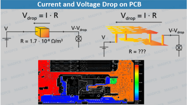
In multilayer boards, interactions between adjacent layers can influence effective resistance, requiring simulation for accurate assessment. Minimizing trace resistance through wider traces reduces voltage drop proportionally, but space constraints demand balanced trade-offs.
Key Factors: Trace Width, Copper Weight, and Current Density
Trace width directly affects cross-sectional area, lowering resistance and allowing higher current without significant voltage drop. Narrow traces increase resistance, amplifying drop under load, while wider ones distribute current more evenly. Copper weight, typically 1 oz/ft2 or 2 oz/ft2, dictates thickness, with heavier copper enabling lower resistance paths for high-current applications. Current density guidelines prevent overheating; exceeding safe levels degrades copper over time via thermal stress.
IPC-2152 provides charts relating current, trace width, copper weight, and allowable temperature rise for precise sizing. Designers select trace width based on maximum expected current and ambient conditions to keep voltage drop under 5% of supply typically. Balancing these factors ensures thermal management alongside electrical performance.
Power Planes for Superior Power Delivery
Power planes offer significantly lower resistance than traces due to their broad area, ideal for distributing power across large board sections. Unlike discrete traces limited by routing space, planes provide uniform voltage with minimal drop, crucial for multi-rail systems. However, splits or slots in planes can create high-impedance paths, necessitating careful partitioning. In high-current designs, combining planes with trace pours enhances current handling while maintaining low inductance.
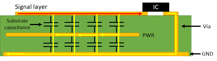
IPC-2221 outlines guidelines for power distribution, recommending plane usage for stability in dense layouts. Planes also act as return paths, reducing loop inductance and improving overall power integrity.
Role of Decoupling Capacitors and Thermal Vias
Decoupling capacitors shunt high-frequency noise to ground, stabilizing the local power supply near IC pins. Placed as close as possible to power pins, they form low-impedance paths that counteract transient voltage drops during switching events. Multiple values in parallel, like 0.1 μF ceramics with bulk electrolytics, cover a broad frequency range effectively. Via placement under capacitors minimizes parasitic inductance, enhancing their decoupling efficacy.
Thermal vias under high-current traces or planes dissipate heat, preventing hotspots that could increase local resistance. Arrays of vias transfer heat to inner layers or the opposite side, maintaining consistent copper performance. These elements collectively address both DC voltage drop and AC noise in power integrity strategies.
Best Practices for PCB Trace Design
Start with accurate current estimates for each net, factoring peak and RMS values to size traces appropriately. Use design rules enforcing minimum trace width based on current density thresholds from standards. Employ heavier copper weight on power layers where feasible, verifying manufacturability. For voltage-sensitive loads, route shortest paths and add redundant vias to reduce effective resistance.
Incorporate power planes for global distribution, stitching them with vias to adjacent ground planes for capacitance. Simulate DC IR drop and AC impedance early, iterating layouts to meet budgets like 3% max drop. Place decoupling capacitors within 1 mm of pins, using blind or buried vias if multilayer constraints apply.
Monitor current density below 0.5 A/mm2 for external layers conservatively, adjusting for internal routing. These practices, aligned with IPC guidelines, yield robust power delivery.
Troubleshooting Common Power Integrity Issues
Engineers often encounter excessive voltage drop in prototypes due to underestimated currents or overlooked trace lengths. Measure drop with scopes under load, comparing to simulations for validation. High current density symptoms include hot spots detectable via thermal imaging; widen traces or add planes as remedies.
Noise from inadequate decoupling appears as jitter on signals; audit capacitor placement and values. Plane splits causing resonances require stitching vias or redesigns. Systematic checks against IPC-2221 ensure resolution without overhauls.
Conclusion
Achieving power integrity demands meticulous attention to trace resistance, trace width, copper weight, and current density. Power planes, decoupling capacitors, and thermal vias form the backbone of stable power delivery, minimizing voltage drop effectively. Adhering to standards like IPC-2152 and IPC-2221 guides engineers toward reliable designs. Implementing these principles enhances PCB performance, reduces failures, and optimizes high-speed systems. Prioritize simulation and verification for success in demanding applications.
FAQs
Q1: How does trace width impact power integrity and voltage drop?
A1: Trace width determines cross-sectional area, directly reducing trace resistance and voltage drop for a given current. Wider traces lower current density, preventing heating and ensuring stable delivery to loads. Per IPC-2152, select widths based on current and temperature rise charts. This maintains voltage within tolerances, critical for sensitive ICs.
Q2: What role do power planes play in minimizing voltage drop?
A2: Power planes provide low-resistance distribution across the board, far superior to traces for high currents. They minimize voltage drop by offering uniform potential and low inductance paths. IPC-2221 recommends planes for power integrity in multilayer designs. Combine with stitching vias for optimal performance.
Q3: Why are decoupling capacitors essential for power integrity?
A3: Decoupling capacitors filter noise and supply transient currents, preventing voltage droop at IC pins. Close placement reduces loop inductance, enhancing effectiveness. Use arrays covering frequency ranges for comprehensive stability. They complement trace design in upholding power integrity.
Q4: How can thermal vias improve high-current PCB traces?
A4: Thermal vias dissipate heat from traces, keeping current density low and resistance stable. They transfer thermal load to other layers, avoiding hotspots. Integrate arrays under power paths for reliability. This supports sustained power delivery without degradation.
References
IPC-2152 — Standard for Determining Current Carrying Capacity in Printed Board Design. IPC, 2009
IPC-2221B — Generic Standard on Printed Board Design. IPC, 2003
IPC-6012E — Qualification and Performance Specification for Rigid Printed Boards. IPC, 2017


