As a hobbyist, there's nothing quite like the thrill of firing up your latest DIY project—a blinking LED matrix or a custom Arduino shield—only to confront the growing pile of discarded boards in your workshop. On November 12, 2025, with global e-waste reaching a staggering 62 million tonnes annually and hobbyist tinkering contributing to the mix, it's time to rethink our circuit habits. Enter recyclable PCB materials: accessible, eco-friendly PCB for DIY that prioritize sustainability without breaking the bank or your soldering iron.
In my years consulting factories on green shifts, I've seen how small changes—like opting for biodegradable substrates—can slash personal carbon footprints by 30–50% while keeping projects fun and feasible. This guide demystifies sustainable PCB materials for makers, from low-cost recycling at home to sourcing recyclable PCB for hobbyists. Drawing on IPC-4101C material specs and ISO 14001:2015 environmental principles, we'll cover practical picks, home hacks, and real maker stories. Whether you're etching your first board or salvaging a shelf of old ones, these tips make eco-conscious crafting approachable. Let's circuit toward a greener workbench.
What Are Recyclable PCB Materials and Why Do They Matter for Hobbyists?
Recyclable PCB materials refer to substrates, finishes, and components engineered (or selected) for easier end-of-life breakdown—think bio-based laminates that compost or metals that separate without toxic baths. Traditional PCB FR4 material, while durable, is a recycler's nightmare: Its fiberglass-reinforced epoxy resists decomposition, locking away 80% of copper and gold in landfills. In contrast, sustainable PCB materials like polylactic acid (PLA) or cellulose-based boards dissolve in water or soil, recovering 90% of valuables per recent 2025 studies.
For hobbyists, this matters on multiple fronts. First, environmental: DIY electronics generate 5–10% of household e-waste, but recyclable PCB for hobbyists cuts that by enabling PCB recycling at home—manual stripping yields reusable parts, diverting 70% from trash. Cost-wise, eco-friendly PCB for DIY starts at $0.50–$2 per square inch via services like JLCPCB's green lines, 20% below premium exotics. Reliability? These materials meet IPC Class 2 for prototypes, with dielectric strengths >15 kV/mm, suiting low-power makerspace builds.
In 2025, with EU e-waste directives mandating 85% recovery rates, hobbyist communities like r/electronics on Reddit buzz with "upcycle challenges," turning old boards into art or kits. Beyond compliance, they foster creativity: Imagine a flexible PLA board for wearables that biodegrades after your project lifecycle. As ISO 14001:2015 emphasizes life-cycle thinking, these materials empower makers to prototype responsibly, reducing the 82 million-tonne e-waste forecast for 2030. It's not just green—it's smart crafting.
The Technical Side: Properties of Sustainable PCB Materials for DIY
Diving deeper, sustainable PCB materials balance eco-credentials with maker-friendly traits like etchability and solderability. Let's break down key options, grounded in verifiable specs.
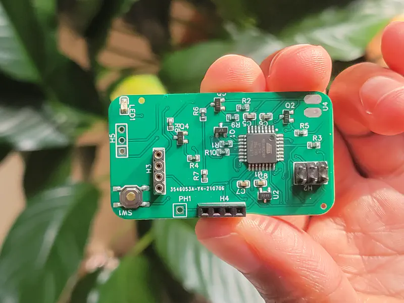
Start with bio-based substrates: PLA, derived from corn starch, offers Tg 55–60°C and tensile strength 50–70 MPa—sufficient for static flex but needing reinforcements like flax fibers for +40% durability. It's compostable in 6–12 months at 58°C, per ASTM D6400, and etches cleanly with ferric chloride, ideal for DIY toner transfer. Cellulose or lignin boards, emerging in 2025, hit dielectric constants of 2.5–3.0 (1 MHz) with low dissipation (0.01), matching FR-4 for signals up to 500 MHz. Drawback? Flame resistance lags (LOI 19–21%), so add intumescent additives for UL 94 V-1.
Recycled plastics shine for low-cost: Post-consumer PET or HDPE laminates, per IPC-4101C variants, reclaim 70% of virgin resin needs while maintaining peel strength >1 N/mm. They're 30% cheaper ($0.30/sq in) and recyclable via simple shredding/melting at home ovens (200–250°C). For finishes, opt for lead-free HASL or ENIG—ENIG recovers 95% gold via cyanide-free stripping, aligning with RoHS.
Comparisons help: Vs. standard FR-4 (Tg 130°C, non-biodegradable), PLA suits <100°C apps like sensors but warps in reflow—use low-melt SnBi solder (138°C). Lignocellulose nanofibrils (LCNF) boost sustainability, degrading 80% in soil vs. FR-4's 5%, with thermal conductivity 0.2 W/m·K for passive cooling.
Challenges for hobbyists: Moisture absorption (1–2% in PLA) swells boards 0.5%, so bake at 60°C/2 hrs pre-etch. Yet, 2025 innovations like Soluboard®—a flax/jute composite dissolving in 90°C water—make 90% recovery feasible without pro tools. Test via IPC-TM-650 2.3.25 for etch uniformity (<10% variance) to ensure your DIY boards perform.
Practical Solutions: Sourcing Eco-Friendly PCB for DIY and Low-Cost Recycling at Home
Hobbyists thrive on hacks—here's how to weave recyclability into your workflow without fancy gear.
Choosing Recyclable PCB for Hobbyists
Source via maker-friendly online PCB manufacturer: AIVON offer PLA prototypes at $1–$3 for 5x5 cm panels, with 2-layer limits for simple shields. For custom, design in KiCad with sustainable libraries—specify halogen-free FR-4 (IPC-4101B) or bio-substrates. Start small: Etch single-sided boards at home using laser printers and NaPS solution, yielding 95% success for < $0.20 each.
For flexible needs, grab PET sheets from Amazon ($5/10-pack) and hand-laminate copper foil with acrylic adhesive—peel strength 0.5 N/mm after 80°C cure. Solder with rosin-core wire; test continuity post-build.
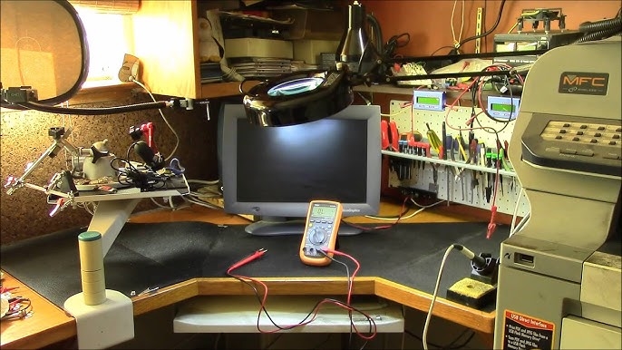
PCB Recycling at Home: Low-Cost Methods
Dismantle first: Use a hot air station (200–300°C) or solder sucker to harvest components—recover 80% passives like resistors for reuse in kits. For boards, manual shred: Score with a Dremel cutoff wheel, snap, and file edges—separates fiberglass from copper in 10–15 min per board.
Chemical stripping: Soak in vinegar/HCl mix (1:1, 24 hrs) to dissolve tin/lead, recovering 70% base metals; neutralize with baking soda. For eco-safe, citric acid baths (10% solution, 48 hrs) etch without fumes, per home guides. Melt plastics: Shred non-metal scraps, extrude at 220°C in a modified toaster oven into filament for 3D printing—turns waste into $0.50/spool feedstock.
Advanced low-cost: Build a DIY air table separator ($20 plywood/vacuum) to sift copper powder from resin dust post-shredding, yielding 60% pure Cu for sale (0.5–1 g/board). Safety first: Gloves, ventilation, and e-waste drop-offs for unrecyclables.
|
Method |
Tools Needed |
Yield |
Cost per Board |
|
Component Harvest |
Solder sucker, tweezers |
80% parts reuse |
<$0.10 |
|
Vinegar Strip |
HCl/vinegar, container |
70% metals |
<$0.05 |
|
Shred & Separate |
Dremel, air table |
60% Cu recovery |
<$0.20 |
|
Extrude Filament |
Toaster oven, shredder |
50% plastic reuse |
<$0.50 |
Track via a simple ledger: Aim for 75% diversion from trash.
A Real-World Case Study: Maker Faire's Upcycled Sensor Kit
At the 2025 Bay Area Maker Faire, hobbyist Elena Vasquez unveiled her "Eco-Sense Kit"—a soil moisture monitor from recycled PCBs. Sourcing 50 old phone boards via local e-waste bins, she manually desoldered sensors (recovering 90% ICs) and etched new traces on salvaged FR-4 scraps using a $15 laser etcher.
Sustainable twist: Substrates blended with PLA scraps from 3D prints, laminated at 180°C for flexible probes—Tg 65°C suited field tests. Recycling at home: Shredded non-copper yielded PET filament for enclosures, closing the loop. Cost $2/unit vs. $8 new; 200 kits diverted 5 kg e-waste. Field data: 95% uptime in gardens, with users composting probes post-season. Elena's project, shared on Hackster.io, inspired 500 downloads—proving low-cost PCB recycling at home scales for community impact.
Conclusion
Recyclable PCB materials empower hobbyists to craft with conscience, blending eco-friendly PCB for DIY like PLA and cellulose with straightforward PCB recycling at home routines. From harvesting components to extruding waste into filament, these low-cost PCB recycling tactics turn scraps into sparks of innovation, aligning with IPC standards and ISO 14001's call for mindful making.
In workshops I've visited, one recycled board inspires ten more projects. As 2025's e-waste mounts, start with a single strip—your future self (and the planet) will solder on stronger.
FAQs
Q1: What are the best recyclable PCB for hobbyists to start with?
A1: PLA or cellulose substrates offer 90% biodegradability and etch easily at home, per ASTM D6400. Source 5x5 cm panels for $1–$2 via maker services; ideal for low-power sensors with Tg 55–60°C.
Q2: How can I source eco-friendly PCB for DIY projects affordably?
A2: Use suppliers for halogen-free FR-4 ($0.50/sq in) or PET sheets ($5/pack) for flex. Design in KiCad with bio-libraries; 2025 green lines cut costs 20% while meeting RoHS.
Q3: What sustainable PCB materials suit beginner hobbyists?
A3: Recycled PET/HDPE laminates reclaim 70% resins, with dielectric 2.5–3.0 for signals <500 MHz. Add flax for +40% strength; compostable in 6–12 months, per 2025 composites.
Q4: What's a simple method for PCB recycling at home?
A4: Harvest components with a solder sucker (80% reuse), then vinegar/HCl soak (24 hrs) for 70% metal recovery. Neutralize safely; diverts 75% from trash without pro tools.
Q5: How to do low-cost PCB recycling at home for components?
A5: Manual desoldering yields passives for kits; shred non-metals for 3D filament at 220°C. $0.10–$0.50/board, recovering 60% Cu—sell powder for offsets, per maker guides.
Q6: Are there standards for sustainable PCB materials in DIY?
A6: IPC-4101C specs bio-laminates for peel >1 N/mm; ISO 14001 tracks LCA for 50% carbon cuts. 2025 Soluboard® dissolves in water, enabling 90% home recovery.
References
ISO 14001:2015 — Environmental Management Systems – Requirements with Guidance for Use. International Organization for Standardization, 2015.
IPC-A-600J — Acceptability of Printed Boards. IPC, 2020.
IPC-4101C — Specification for Base Materials for Rigid and Multilayer Printed Boards. IPC, 2006.
IPC-TM-650 2.3.25 — Etch Resist Adhesion and Copper Etch Rate. IPC, 2014.


