Introduction
Electromagnetic interference, commonly known as EMI, poses a significant challenge in PCB prototyping. It can disrupt signal integrity, affect performance, and lead to compliance issues with regulatory standards. For electrical engineers, mitigating EMI during the design and prototyping phase is critical to ensure reliable functionality. This article explores practical methods for reducing EMI through effective PCB EMI shielding and grounding strategies. It also covers essential techniques like signal filtering, common mode choke integration, and ferrite bead placement on PCBs. By applying these strategies early in the design process, engineers can minimize interference risks and enhance product reliability. The focus remains on actionable insights grounded in industry practices, helping professionals tackle EMI challenges systematically.
What Is EMI and Why It Matters in PCB Design
EMI refers to the disturbance caused by electromagnetic fields that interfere with electronic circuits. In PCB design, EMI can originate from internal sources like high-speed signals or external sources such as nearby devices. This interference can degrade signal quality, cause data errors, or lead to system failures. For electrical engineers, addressing EMI is vital to meet electromagnetic compatibility requirements as outlined in standards like IEC 61000. Failure to control EMI can result in costly redesigns or non-compliance with regulations. Moreover, in applications like medical or automotive electronics, EMI can pose safety risks. Understanding and mitigating EMI during PCB prototyping ensures that the final product performs as intended in real-world conditions.
Technical Principles of EMI in PCBs
EMI in PCBs primarily arises from two mechanisms: conducted interference and radiated interference. Conducted EMI travels through power lines or signal traces, often due to switching noise or crosstalk. Radiated EMI, on the other hand, propagates through the air as electromagnetic waves, typically from high-frequency signals or poorly shielded components.
The root cause often lies in loop areas formed by signal paths and their return currents. Larger loop areas act as antennas, amplifying radiated emissions. Additionally, improper grounding can create potential differences, leading to common mode noise. High-speed digital signals with fast rise times contribute significantly to EMI by generating harmonics that interfere with nearby circuits. Understanding these principles helps engineers identify critical areas in a PCB layout where EMI is likely to occur.
Another key factor is the coupling between traces. Capacitive and inductive coupling between adjacent traces can introduce noise, especially in densely packed designs. Power supply noise also plays a role, as fluctuations can propagate through the board and affect sensitive components. Standards such as IEC 61000-4-2 provide guidelines on testing and limits for EMI susceptibility, offering a benchmark for design validation.
Practical Solutions for Reducing EMI in PCB Prototyping
Effective Grounding Strategies for PCBs
Grounding is a fundamental aspect of EMI control in PCB design. A well-designed ground plane minimizes loop areas and provides a low-impedance path for return currents. One key grounding strategy for PCBs is to use a continuous ground plane on multilayer boards. This reduces the risk of ground loops and ensures uniform potential across the board. For two-layer designs, creating a grid of ground traces can approximate a ground plane's benefits.
Another important practice is to separate analog and digital grounds. Connecting them at a single point near the power supply prevents noise from digital circuits from affecting analog sections. Additionally, placing decoupling capacitors close to IC power pins helps suppress high-frequency noise on the ground plane. Engineers should also avoid splitting ground planes under high-speed signal traces, as this disrupts return paths and increases EMI.
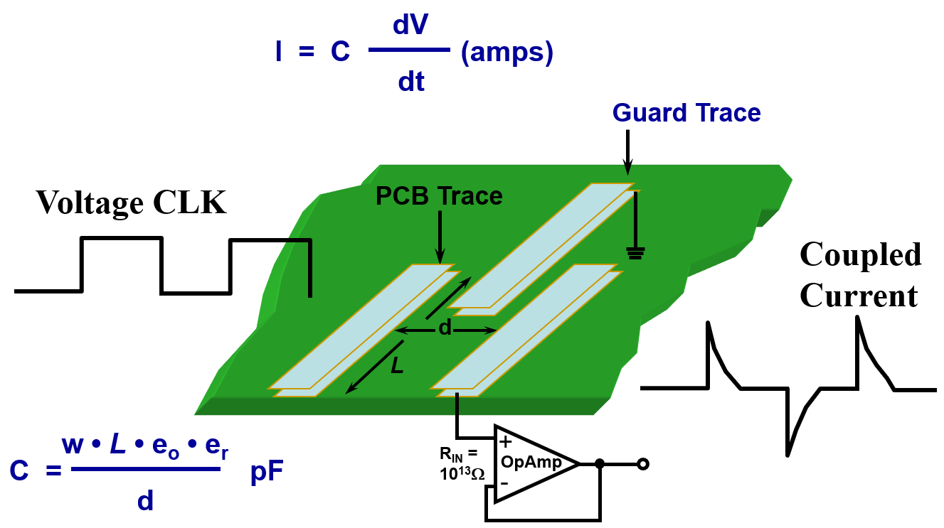
PCB EMI Shielding Techniques
Shielding is a direct method to block radiated EMI. PCB EMI shielding involves enclosing sensitive areas or components with conductive materials to prevent electromagnetic fields from penetrating or escaping. One common approach is to use metal enclosures or cans over critical components like RF modules. These shields must be connected to the ground plane to be effective.
In multilayer PCBs, internal ground planes can act as shields between signal layers, reducing crosstalk and radiated emissions. Designers can also implement guard traces, which are grounded traces placed between high-speed signals to isolate them. For prototyping, temporary shielding using conductive tapes or foils can help identify EMI sources before finalizing the design. Following guidelines from standards like IEC 61000-4-3 ensures that shielding meets radiated immunity requirements.
Signal Filtering Techniques for PCBs
Signal filtering techniques for PCBs are essential to suppress conducted EMI. Filters remove unwanted high-frequency noise from power and signal lines. Low-pass filters, for instance, can be used on signal lines to attenuate harmonics generated by fast-switching circuits. Placing these filters close to the noise source or sensitive component maximizes their effectiveness.
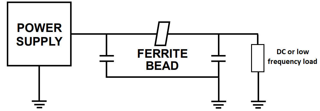
A common mode choke on a PCB is another powerful tool for EMI reduction. It blocks common mode noise while allowing differential signals to pass through. These chokes are particularly useful in power supply lines or interfaces like USB, where external noise is a concern. Proper selection of the choke based on current rating and frequency response is critical for optimal performance.
Ferrite bead placement on a PCB also plays a significant role in filtering. Ferrite beads act as high-frequency resistors, dissipating noise as heat. They should be placed close to the power pins of ICs, paired with a decoupling capacitor to form a pi-filter configuration. This setup effectively reduces power supply noise. Engineers must ensure that the bead's impedance matches the frequency range of the noise being targeted.
Layout Optimization for EMI Control
PCB layout directly influences EMI performance. Minimizing trace lengths for high-speed signals reduces loop areas and potential radiation. Routing differential pairs closely together maintains signal integrity and cancels out common mode noise. Additionally, avoiding right-angle bends in traces prevents impedance discontinuities that can cause reflections and emissions.
Power and ground planes should be placed adjacent to each other in multilayer boards to create a low-inductance path for return currents. This arrangement also enhances decoupling capacitor effectiveness. Keeping clock signals away from board edges prevents them from radiating as antennas. Adhering to layout guidelines in standards like IPC-2221B ensures that designs are optimized for EMI reduction from the start.
Troubleshooting EMI Issues in Prototyping
During PCB prototyping, identifying and resolving EMI issues early saves time and resources. One common problem is excessive radiated emissions from high-speed traces. Using a near-field probe, engineers can locate emission hotspots and adjust the layout or add shielding as needed. Another frequent issue is conducted noise on power lines, often due to inadequate decoupling. Adding capacitors or ferrite beads near affected components can resolve this.
Ground bounce, caused by simultaneous switching of multiple outputs, is another challenge. It can be mitigated by increasing ground plane coverage or using lower-speed drivers if possible. Testing prototypes under conditions outlined in IEC 61000-4-6 for conducted immunity helps validate designs against real-world interference. Documenting test results and iterating on the layout ensures continuous improvement in EMI performance.
Conclusion
Reducing EMI in PCB prototyping requires a combination of strategic design and practical implementation. Grounding strategies for PCBs, such as continuous ground planes and single-point connections, form the foundation of EMI control. PCB EMI shielding techniques, including metal cans and guard traces, protect sensitive areas from interference. Signal filtering techniques for PCBs, like common mode chokes and ferrite bead placement, address conducted noise effectively. By integrating these methods into the design process, electrical engineers can achieve robust prototypes that meet regulatory standards and perform reliably. Early attention to EMI ensures smoother transitions from prototyping to production, minimizing costly revisions.
FAQs
Q1: How do grounding strategies for PCBs reduce EMI?
A1: Grounding strategies for PCBs minimize EMI by providing a low-impedance path for return currents, reducing loop areas that act as antennas. A continuous ground plane prevents potential differences and ground loops. Separating analog and digital grounds with a single connection point avoids noise crossover. Following guidelines from standards like IEC 61000 ensures effective grounding for improved signal integrity and reduced interference.
Q2: What is the role of a common mode choke on a PCB in EMI reduction?
A2: A common mode choke on a PCB blocks common mode noise while allowing differential signals to pass, making it ideal for power lines or data interfaces. It suppresses interference from external sources or internal switching noise. Proper selection based on current and frequency range is essential. This component significantly reduces conducted EMI when placed strategically near noise entry points.
Q3: Where should ferrite bead placement on a PCB be for optimal EMI filtering?
A3: Ferrite bead placement on a PCB should be close to the power pins of integrated circuits to filter high-frequency noise effectively. Pairing it with a decoupling capacitor forms a pi-filter, enhancing noise suppression. Correct positioning ensures that power supply noise is dissipated before reaching sensitive components. This setup is critical for maintaining clean power delivery in high-speed designs.
Q4: What are key signal filtering techniques for PCBs to control EMI?
A4: Signal filtering techniques for PCBs include using low-pass filters on signal lines to remove high-frequency harmonics. Ferrite beads and common mode chokes address power line noise. Placing filters near noise sources or sensitive areas maximizes effectiveness. These methods, aligned with standards like IEC 61000-4-6, help engineers control conducted EMI and ensure reliable circuit performance during prototyping.
References
IEC 61000-4-2:2008 — Electromagnetic Compatibility (EMC) - Part 4-2: Testing and Measurement Techniques - Electrostatic Discharge Immunity Test. IEC, 2008.
IEC 61000-4-3:2020 — Electromagnetic Compatibility (EMC) - Part 4-3: Testing and Measurement Techniques - Radiated, Radio-Frequency, Electromagnetic Field Immunity Test. IEC, 2020.
IEC 61000-4-6:2013 — Electromagnetic Compatibility (EMC) - Part 4-6: Testing and Measurement Techniques - Immunity to Conducted Disturbances, Induced by Radio-Frequency Fields. IEC, 2013.
IPC-2221B:2012 — Generic Standard on Printed Board Design. IPC, 2012.


