What is RF PCB Design and Why is it Critical for Modern Electronics?
Radio Frequency (RF) Printed Circuit Board (PCB) design is the specialized process of crafting circuit boards capable of handling high-frequency signals, typically ranging from 3 kHz to 300 GHz. These PCBs are fundamental to a vast array of contemporary technologies, including wireless communication systems, radar, GPS devices, and various internet-of-things (IoT) applications. Unlike conventional PCB design, RF PCB development demands meticulous attention to signal integrity, precise impedance matching, and stringent control over electromagnetic interference (EMI) due to the inherently high-frequency nature of the signals involved.
The significance of expertly executed RF PCB design cannot be overstated, as it directly influences device performance. A suboptimal RF PCB can lead to substantial signal degradation, increased noise, or even complete operational failure of the electronic system. For those embarking on their journey into electronics, mastering the foundational principles of RF PCB design ensures that their creations will function dependably in real-world scenarios, whether constructing a basic radio or an intricate IoT device.
Initial Hurdles in RF PCB Design
Before delving deeper, it’s helpful to acknowledge common challenges that beginners in RF PCB design often face:
● Signal Integrity: High-frequency signals are highly susceptible to distortion and loss if the conductive traces on the board are not designed with extreme precision.
● Impedance Matching: Discrepancies in impedance can cause signals to reflect rather than transfer efficiently. A typical target impedance for RF traces is 50 ohms.
● EMI and Noise: RF circuits are inherently sensitive to interference, whether originating from adjacent components on the board or from external electromagnetic sources.
● Material Selection: Standard PCB base materials may prove inadequate at high frequencies, often necessitating the use of specialized substrates like those from Rogers Corporation or PTFE-based laminates.
Grasping the Core Theories Behind RF PCB Design
To truly excel in designing RF PCBs, a foundational understanding of the theories governing high-frequency circuits is indispensable. This section aims to provide an accessible introduction to these complex concepts for beginners.
Understanding Radio Frequency Signals
RF signals are a form of electromagnetic wave characterized by their rapid oscillations. Unlike lower-frequency electrical currents, RF signals exhibit distinct wave-like properties, meaning they can radiate energy into their surroundings and potentially interfere with other signals. This wave behavior is precisely why RF PCB design places such a heavy emphasis on meticulously controlling trace dimensions—including length, width, and spacing—to prevent signal reflections and minimize energy loss.
The Criticality of Impedance Matching
Impedance represents the opposition a circuit presents to the flow of alternating current. In RF engineering, ensuring that the impedance of the signal source, the transmission line (the PCB trace), and the load (the receiving component) are all perfectly matched (commonly to 50 ohms) is paramount. This matching maximizes the transfer of power and significantly reduces signal reflections. For example, a mismatch can result in a Standing Wave Ratio (SWR) greater than 1:1, directly leading to power inefficiency and signal degradation.
Signal Propagation and Skin Effect Phenomena
At higher frequencies, electrical current does not uniformly distribute throughout the entire cross-section of a conductor. Instead, it tends to flow predominantly along the surface of the conductor, a phenomenon known as the skin effect. Consequently, simply making traces wider does not always translate to better performance for RF signals. Designers must carefully calculate trace widths based on the operational frequency—for instance, 2.4 GHz for Wi-Fi applications—to ensure minimal signal loss due to this effect.
Related Reading: Advanced RF PCB Routing Techniques: Mastering Microstrips and Striplines
Fundamental Principles of RF PCB Design for Beginners
With a grasp of the underlying theory, let's transition to the practical, foundational principles of RF PCB design. These guidelines form the bedrock of any effective RF PCB design tutorial or course.
Selecting Appropriate Board Materials
Conventional FR-4 material, widely used in low-frequency PCBs, often proves unsuitable for RF applications due to its relatively high dielectric constant and loss tangent, which can cause significant signal attenuation at radio frequencies. For RF designs, materials such as Rogers 4350B (with a dielectric constant of approximately 3.48) or laminates based on PTFE are often preferred. These specialized materials offer superior low-loss characteristics and stable performance, especially at frequencies exceeding 1 GHz.
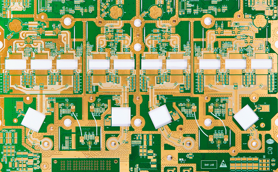
Strategic Layer Stack-Up Design
RF PCBs commonly employ multi-layer constructions to effectively isolate sensitive signal layers from ground and power planes. A typical four-layer stack-up might be configured as follows:
● Top Layer: Dedicated to RF traces and surface-mounted components.
● Layer 2: A solid ground plane, crucial for shielding and providing a return path.
● Layer 3: A power plane, distributing necessary voltages.
● Bottom Layer: Can be used for additional routing, less sensitive signals, or another ground plane.
This layered approach minimizes interference and establishes a stable, low-impedance reference for RF signals.
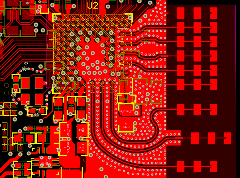
Meticulous Trace Design and Routing
In RF PCB design, routing traces involves far more than just connecting two points. Careful consideration must be given to:
● Trace Width: Precisely calculated to achieve the desired characteristic impedance, typically 50 ohms for RF transmission lines.
● Trace Length: Should be kept as short as possible to mitigate signal delay and loss. A signal traveling at 1 GHz, for example, traverses only about 15 cm in a nanosecond on a standard PCB.
● Corner Management: Avoid sharp 90-degree bends; instead, use smooth 45-degree angles or curved traces to prevent signal reflections that can degrade performance.
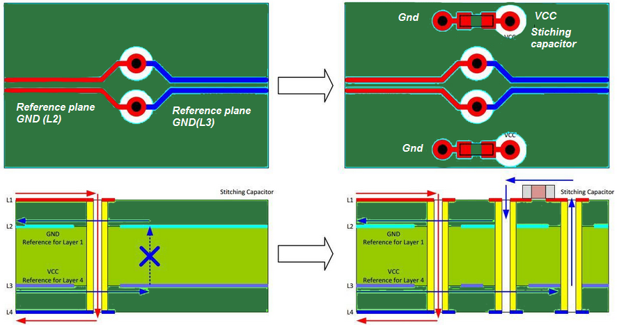
Implementing Robust Ground Planes and Shielding
A continuous, uninterrupted ground plane is absolutely critical in RF PCB design. It provides a low-impedance return path for high-frequency signals and significantly reduces electromagnetic interference. It is imperative to avoid segmenting the ground plane directly beneath RF traces, as such breaks can create unintended resonant loops that act as antennas, potentially introducing unwanted noise and coupling.
Related Reading: Multilayer PCB Design for RF Applications: Optimizing Performance at High Frequencies
A Practical Walkthrough: Step-by-Step RF PCB Design for Newcomers
This section offers a practical RF PCB design tutorial, guiding you through the essential stages of developing your initial high-frequency circuit board.
Step 1: Define Your Project Specifications
Begin by clearly outlining the key operational parameters of your circuit. This includes the intended operating frequency, necessary power levels, and the specific application. For instance, a 2.4 GHz Wi-Fi module will have distinct requirements compared to a 900 MHz RFID system. Document critical parameters such as the target impedance (usually 50 ohms) and acceptable maximum signal loss (often specified as less than 3 dB).
Step 2: Select Appropriate Software Tools
Choose a PCB design software that provides capabilities for RF simulations and precise impedance calculations. Numerous free or affordably priced tools are available online, offering functionalities like schematic capture and layout design. Look for software that includes integrated calculators to determine optimal trace widths and spacings based on your specified operating frequency and material properties.
Step 3: Develop the Circuit Schematic
Create a detailed schematic of your circuit, incorporating all necessary RF components such as amplifiers, filters, and antenna matching networks. Crucially, ensure the inclusion of decoupling capacitors strategically placed near power pins to suppress high-frequency noise—typically, 0.1 μF capacitors are used for high-frequency applications.
Step 4: Design the Physical Layout
Translate your schematic into a physical PCB layout, diligently adhering to the trace routing and ground plane principles discussed earlier. While vias are necessary for connecting different layers, minimize their use within critical RF signal paths to avoid introducing unwanted inductance and impedance discontinuities.
Step 5: Simulate and Validate the Design
Prior to initiating manufacturing, perform thorough simulations of your design to verify signal integrity and confirm accurate impedance matching. Advanced simulation tools often provide S-parameter analysis, which can predict how your circuit will perform at the intended operating frequencies, for example, at 5 GHz for certain wireless applications.
Step 6: Prototype, Test, and Refine
Once your design has been simulated and validated, proceed to manufacture a prototype. Rigorously test this prototype using specialized equipment, such as a vector network analyzer (VNA), to measure key performance indicators like return loss. If the test results do not meet your specified requirements—for instance, if the return loss is worse than -10 dB—then revise the layout accordingly and repeat the testing process until optimal performance is achieved.
Common Pitfalls and How to Navigate Them in RF PCB Design
As a beginner, making mistakes in RF PCB design is a natural part of the learning process. Recognizing common pitfalls and understanding how to circumvent them can significantly accelerate your progress.
Overlooking Impedance Control
A frequent error is neglecting to accurately calculate the trace width required to maintain a 50-ohm impedance. This oversight inevitably leads to signal reflections and degraded performance. Always leverage online calculators or software tools to precisely determine the correct trace dimensions based on your board's dielectric constant and thickness.
Inadequate Grounding Practices
Poor grounding, characterized by split ground planes or an insufficient number of ground vias, can severely compromise signal integrity by introducing unwanted noise and crosstalk. Always implement a continuous, solid ground plane and strategically place vias to ensure robust, low-impedance connections between ground layers.
Related Reading: RF PCB Via Design: Minimizing Inductance and Maximizing Signal Integrity
Suboptimal Component Placement
Placing sensitive RF components in close proximity to noisy digital circuits can lead to significant interference. It is best practice to group all RF components together, forming a dedicated RF section, and to isolate this area from digital or power sections through physical separation, ground fills, or, when necessary, dedicated shielding structures.
Online Resources for Learning RF PCB Design
For individuals seeking an RF PCB design course or alternative ways to learn RF PCB design online, a wealth of resources is available to help cultivate and enhance your skills.
Free Tutorials and In-depth Guides
Numerous websites offer complimentary RF PCB design tutorials that encompass everything from theoretical concepts to practical layout recommendations. Seek out step-by-step guides that include tangible examples, such as the design of a simple RF amplifier circuit.
Structured Video Courses
Online platforms like YouTube host extensive video series specifically tailored for beginners in RF PCB design. These courses often feature visual demonstrations of design software tools and walk-throughs of real-world projects, making complex subjects more accessible and easier to comprehend.
Engaging with Community Forums
Participate in online communities and forums where experienced engineers readily share their insights and offer advice on various RF PCB design challenges. These platforms are invaluable for troubleshooting specific issues, such as effectively reducing electromagnetic interference in a 433 MHz circuit, and for networking with peers.
Essential Tips for Success in RF PCB Design
To conclude this RF PCB design tutorial, here are some final pieces of advice to guide your journey and foster success as a beginner:
● Start Simple: Begin with less complex projects, such as designing a low-power RF transmitter, before attempting more intricate and demanding designs.
● Master Software Tools: Dedicate time to thoroughly learn your chosen PCB design software. These tools are invaluable for automating crucial tasks like impedance calculations and complex simulations.
● Stay Informed: Regularly keep abreast of evolving industry standards and best practices pertinent to RF design, particularly those related to common wireless protocols like Bluetooth or Zigbee.
● Collaborate and Seek Feedback: Actively engage with experienced designers through online platforms or professional networks to gain valuable insights, receive constructive feedback, and continuously refine your design methodologies.
Conclusion
While RF PCB design might initially appear challenging for beginners, acquiring the correct foundational knowledge transforms it into an attainable and rewarding skill. This guide has meticulously covered the core principles of RF PCB design basics, ranging from understanding high-frequency theory to applying practical layout techniques. Whether you choose to follow a structured RF PCB design course, explore online learning platforms, or utilize this tutorial as your initial springboard, remember that consistent practice and unwavering patience are paramount to your development.
By concentrating your efforts on achieving excellent signal integrity, precise impedance matching, and implementing robust grounding strategies, you will be well-equipped to create dependable RF circuits for a broad spectrum of applications. Begin with modest projects, conduct frequent testing, and commit to continuous learning to progressively refine your expertise in RF PCB design. With these essential tools and accumulated knowledge, you are poised to master the fascinating realm of high-frequency electronics.


