Introduction
In high-speed PCB designs, crosstalk poses a significant challenge to signal integrity, particularly in sensitive circuits handling RF signals or multi-gigabit data rates. Crosstalk occurs when electromagnetic interference from one trace affects adjacent signals, leading to noise, timing errors, and degraded performance. PCB shielding crosstalk mitigation becomes essential to maintain reliable operation in applications like telecommunications, automotive electronics, and medical devices. Engineers must employ targeted shielding strategies to minimize this unwanted coupling without compromising board compactness or cost. This article explores effective crosstalk shielding techniques, from fundamental principles to practical implementations, helping designers achieve optimal shielding effectiveness crosstalk. By understanding these methods, teams can enhance overall system reliability.
What Is Crosstalk and Why It Matters in Sensitive Circuits
Crosstalk refers to the unintentional transfer of signals between adjacent conductors on a PCB, primarily through capacitive and inductive coupling. Capacitive crosstalk arises from electric fields between parallel traces, while inductive crosstalk stems from magnetic fields generated by changing currents. In sensitive circuits, such as those in high-frequency analog or mixed-signal boards, even low-level crosstalk can distort critical signals, causing bit errors or reduced dynamic range. For electric engineers, recognizing crosstalk's impact is crucial during the design phase, as it directly influences compliance with signal integrity budgets.
The relevance of crosstalk grows with increasing data rates and shrinking geometries in modern PCBs. As trace spacing narrows to fit more I/O in dense layouts, coupling intensifies, potentially violating timing margins or introducing jitter. Sensitive circuits, like those in ADCs or SerDes interfaces, demand crosstalk below microvolt levels to preserve accuracy. Without proper PCB shielding crosstalk measures, systems may fail electromagnetic compatibility tests or exhibit intermittent failures in the field. Addressing this early prevents costly respins and ensures robust performance across operating conditions.
Technical Principles of Crosstalk in PCBs
Crosstalk mechanisms follow well-established electromagnetic principles, governed by mutual capacitance and inductance between traces. For capacitive coupling, the voltage induced on a victim trace is proportional to the aggressor's dv/dt, with coupling strength depending on trace overlap area, separation, and dielectric constant. Inductive coupling, conversely, scales with di/dt and mutual inductance, which increases with parallel run lengths and proximity. Near-end crosstalk (NEXT) appears at the source end of the victim, while far-end crosstalk (FEXT) propagates to the receiver, complicating mitigation.
Key factors amplifying crosstalk include fast signal rise times, long parallel trace runs, and impedance mismatches. In multilayer boards, coupling extends through planes if return paths are inadequate, creating ground bounce that exacerbates noise. Shielding effectiveness crosstalk hinges on breaking these field lines, either by physical barriers or field cancellation. Engineers model these using field solvers, but analytical approximations from transmission line theory provide quick insights during layout reviews. Understanding these principles guides the selection of appropriate crosstalk shielding techniques.
Dielectric materials and stackup configurations also influence coupling coefficients. Thinner dielectrics boost capacitance per unit length, while high-frequency laminates with lower loss tangents help but do not eliminate crosstalk. Ground reference planes act as virtual shields by providing low-impedance return paths, reducing loop areas for magnetic fields. However, plane splits or slots can create resonances that worsen coupling at specific frequencies.
Related Reading: The Impact of Impedance Control on Crosstalk: A Comprehensive Analysis
Crosstalk Shielding Techniques: Core Strategies
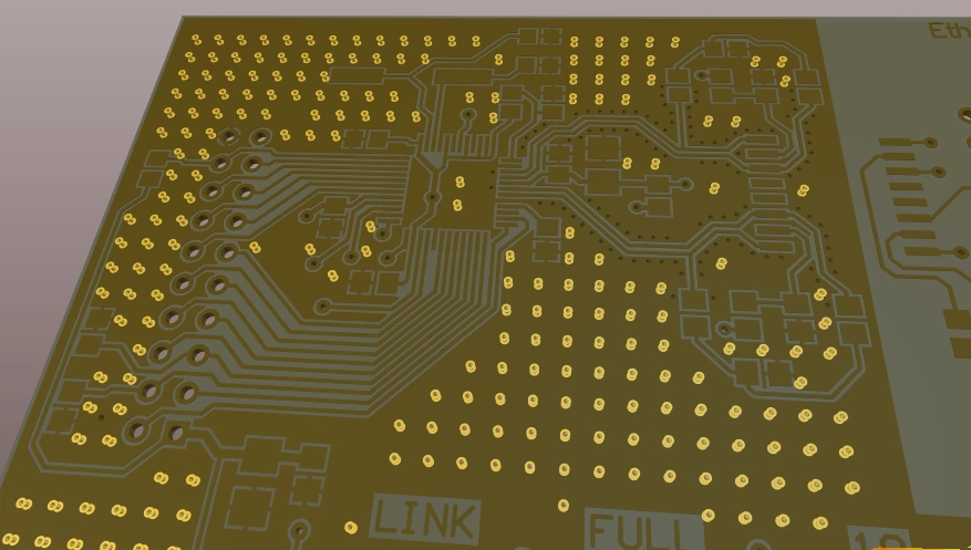
Effective PCB shielding crosstalk relies on a hierarchy of techniques, starting with layout optimizations and progressing to dedicated shielding structures. The simplest approach involves increasing trace spacing and minimizing parallel lengths, guided by rules like 3W spacing for high-speed signals, where W is trace width. Guard traces, grounded on both sides, intercept fields from aggressors, offering up to 20 dB reduction in coupling without adding layers. These dual-purpose traces also serve as stitching points for planes.
Ground planes form the backbone of crosstalk shielding techniques, confining fields between signal and reference layers. Full ground pours on inner layers image signals, halving effective coupling by symmetric field distribution. Vias placed along trace edges, known as via fencing or stitching, connect planes and block slot modes that propagate noise. Spacing vias at lambda/20, where lambda is the wavelength, ensures continuous shielding up to gigahertz frequencies. This method aligns with IPC guidelines for controlled impedance and signal integrity.
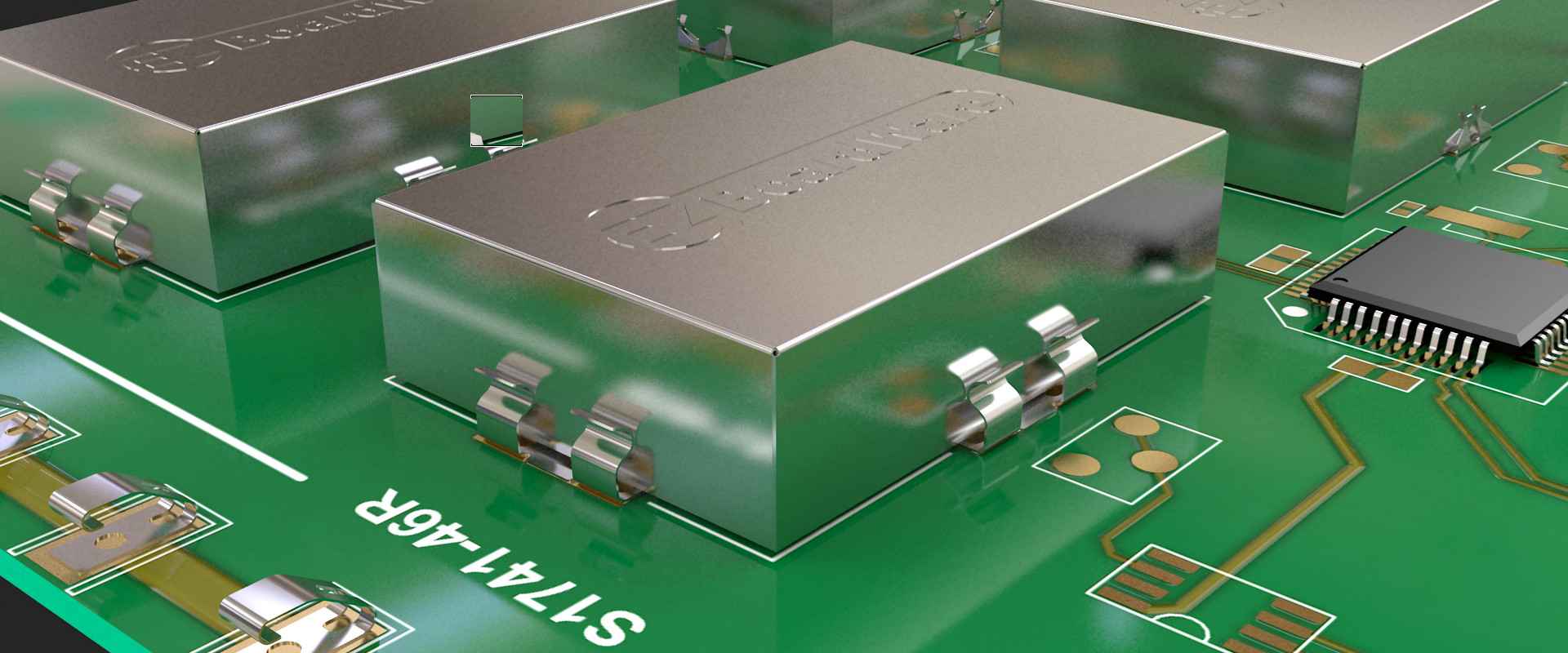
For extreme cases in sensitive circuits, shielding cans or enclosures encapsulate noisy sections, providing Faraday cage-like isolation. These metal covers, soldered or clipped to ground, achieve shielding effectiveness crosstalk exceeding 40 dB, ideal for RF modules. Partial shielding with grounded copper pours around traces offers a cost-effective alternative, though care must be taken to avoid resonances from enclosed cavities. Combining these with differential routing further suppresses common-mode coupling.
Advanced Shielding Implementations and Stackup Design
Multilayer stackups amplify shielding effectiveness crosstalk through dedicated shield layers. Embedding a ground plane immediately adjacent to signal layers minimizes loop inductance, while power planes with decoupling capacitors act as partial shields. Microstrip configurations outperform stripline for low crosstalk at the expense of radiation, so engineers balance based on board constraints. Asymmetric stackups, with ground over signal layers, reduce broadside coupling between layers.
Via shielding extends to inter-layer transitions, where blind or buried vias fenced by ground vias prevent coupling through clearance holes. In HDI boards, finer pitches demand denser stitching, often every 1-2 mm. Compliance with IPC-6012 standards ensures these features maintain integrity post-fabrication. Simulations validate designs, correlating coupling to S-parameters like S31 for NEXT.
Embedded shielding films or conductive pastes represent emerging crosstalk shielding techniques, applied selectively to high-risk areas. These conform to irregular surfaces, unlike rigid cans, and integrate seamlessly in assembly. Thermal management remains key, as shields can trap heat, necessitating vents or heat sinks.
Related Reading: Crosstalk in High Speed Digital Design: Challenges and Solutions
Troubleshooting Common Crosstalk Issues
Engineers often encounter crosstalk in prototypes despite simulations, due to unmodeled effects like via parasitics or board warpage altering clearances. Probing with near-field scanners reveals hotspots, guiding targeted fixes like added stitching. If ground planes resonate, adjusting via density or adding lossy materials dampens modes. Pre-layout checklists, including length matching and impedance control per J-STD-001, prevent recurrence.
In mixed-signal boards, analog sections require moats or isolated grounds to block digital noise spillover. Measuring shielding effectiveness crosstalk via TDR or VNA confirms improvements, targeting < -40 dB isolation. Iterative prototyping refines techniques, ensuring field performance matches lab results.
Case Insights: High-Speed SerDes Implementation
Consider a 56 Gbps SerDes channel on a 12-layer board, where initial crosstalk exceeded 5% of eye height. Implementing dual ground planes with 1 mm via stitching reduced NEXT by over 15 dB, restoring margins. Guard rings around TX/RX pairs further isolated channels. This approach, rooted in transmission line shielding principles, scaled to full backplanes without respins.
Conclusion
Mastering PCB shielding crosstalk demands a blend of layout discipline, stackup optimization, and targeted structures like guard traces and via fencing. These crosstalk shielding techniques deliver measurable shielding effectiveness crosstalk, safeguarding sensitive circuits from noise degradation. Electric engineers benefit from early integration, aligning with standards for reproducible results. Prioritizing signal integrity through these strategies ensures reliable, high-performance designs. Future trends in 3D packaging will evolve these methods, but fundamentals remain timeless.
FAQs
Q1: What are the most effective PCB shielding crosstalk techniques for high-speed designs?
A1: Guard traces, ground plane stitching via vias, and dedicated shield layers top the list for crosstalk shielding techniques. These interrupt electric and magnetic fields, achieving 20-50 dB isolation depending on frequency. Implement spacing rules and simulate before layout to maximize shielding effectiveness crosstalk. Compliance with IPC standards ensures fabrication consistency.
Q2: How does via fencing improve shielding effectiveness crosstalk?
A2: Via fencing connects ground planes along signal paths, blocking slotline modes and reducing inductive coupling. Place vias at quarter-wavelength intervals for broadband performance. This technique enhances PCB shielding crosstalk in multilayer boards, often cutting noise by 10-30 dB. Verify with S-parameter measurements post-assembly.
Q3: Why do ground planes excel in crosstalk shielding techniques?
A3: Ground planes provide low-impedance returns and image signals to confine fields, minimizing loop areas. Full pours outperform partitioned ones for broad frequency coverage. In sensitive circuits, they form the foundation of shielding effectiveness crosstalk strategies. Pair with decoupling for optimal results.
Q4: When should engineers prioritize crosstalk shielding techniques in PCB design?
A4: Prioritize during schematic and stackup planning for data rates above 10 Gbps or RF above 1 GHz. Sensitive circuits like ADCs demand it to meet noise budgets. Assess via coupling budgets early to select appropriate PCB shielding crosstalk methods.
References
IPC-2221B — Generic Standard on Printed Board Design. IPC, 2009
IPC-6012E — Qualification and Performance Specification for Rigid Printed Boards. IPC, 2017
J-STD-001H — Requirements for Soldered Electrical and Electronic Assemblies. IPC, 2018