Introduction
In high-frequency PCB design, maintaining signal integrity backdrilling techniques emerge as a critical strategy for PCB performance optimization. Engineers face persistent challenges from via stubs that degrade signals at gigabit speeds and beyond. These stubs introduce reflections and distortions that compromise data transmission reliability. Backdrilling addresses these issues by precisely removing excess via material, enabling cleaner signal paths. This approach proves essential for applications demanding robust high-frequency PCB operation, such as telecommunications and computing systems. Understanding backdrilling unlocks superior performance in complex multilayer boards.
What Is Backdrilling and Why It Matters for Signal Integrity
Backdrilling involves a secondary drilling process on through-hole vias to eliminate the unused stub portion extending beyond the signal layers. This technique targets the non-functional copper barrel that remains after initial plating in multilayer PCBs. Without backdrilling, these stubs act as resonant elements, particularly detrimental in high-frequency environments. Signal integrity backdrilling directly counters via resonance, a common culprit in signal degradation. For electric engineers designing high-speed interfaces, ignoring stub effects risks eye closure and bit error rates climbing unacceptably. IPC-6012 outlines qualification requirements for such advanced via structures, emphasizing their role in performance specifications.
The relevance intensifies with rising data rates in modern electronics. High-frequency PCBs operating above several gigahertz suffer impedance mismatches from via stubs, leading to return loss and insertion loss spikes. Backdrilling restores continuity in the transmission line model of the via. This optimization aligns with the demands of protocols requiring low jitter and high bandwidth. Engineers benefit from reduced simulation iterations when incorporating backdrilling early in the design phase. Ultimately, it elevates PCB performance optimization from theoretical to practical reliability.
Related Reading: Backdrilling Design: A Beginner's Guide to Reducing Signal Reflections in PCBs
Technical Principles Behind Via Resonance and Impedance Discontinuities
Via resonance occurs when the stub length approaches a quarter wavelength of the signal frequency, turning the stub into an open-circuited transmission line. At resonance, the stub reflects energy back toward the source, causing severe signal distortion. This phenomenon manifests as periodic notches in the frequency response, directly impacting high-frequency PCB integrity. Impedance matching falters because the via stub introduces a capacitive discontinuity followed by inductive behavior. Engineers model these effects using time-domain reflectometry or S-parameter simulations to quantify the degradation. The shorter the stub, the higher the frequency at which resonance shifts out of the operational band.
Impedance discontinuities from vias compound these issues in dense routing. A standard through-via presents varying characteristic impedance along its length due to the stub's geometry. This variation causes mode conversion in differential pairs, converting common-mode noise into differential signals. Via resonance exacerbates crosstalk between adjacent vias, especially in fanout regions from BGA packages. High-frequency signals experience greater attenuation as energy couples to unwanted modes. Backdrilling mitigates these by tailoring the via to the active layers, creating a more uniform impedance profile.
Transmission line theory underpins the need for stub removal. The reflection coefficient at the stub end equals 1 for an open circuit, sending a full wave back. For signals where stub length exceeds skin depth effects, this reflection arrives delayed, smearing the eye pattern. Impedance matching requires the via's effective length to minimize phase shifts. In multilayer stacks, core and prepreg thicknesses dictate stub lengths, often spanning multiple dielectric layers. Precise control over backdrill depth ensures the remaining barrel aligns with signal paths.
How Backdrilling Optimizes Signal Integrity
Backdrilling enhances signal integrity backdrilling by shortening the via stub to negligible lengths relative to the wavelength. This shift pushes resonance frequencies well beyond the PCB's operating range, flattening the insertion loss curve. Engineers observe improved return loss, often exceeding 20 dB across broader bandwidths post-backdrilling. The process preserves plating integrity on active segments while cleanly excising the stub. IPC-2221 provides design guidelines for managing such via discontinuities in high-speed boards. This standard reinforces the engineering rationale for controlled depth drilling.
Impedance matching improves as the backdrilled via approximates a coaxial transmission line over its functional length. The larger backdrill diameter creates an annular gap, reducing parasitic capacitance. This adjustment allows better tuning to the trace impedance, typically 50 ohms single-ended or 100 ohms differential. High-frequency PCB designs benefit from wider eye openings and reduced jitter. Simulations confirm lower total channel loss when combining backdrilling with optimized stackups. Practical implementations show enhanced margins for routing longer traces.
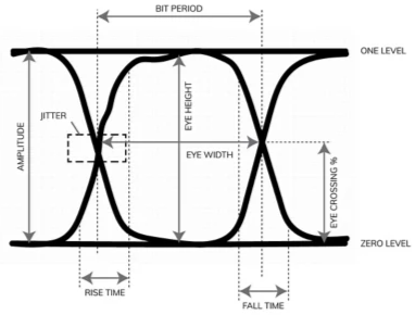
Signal propagation delays minimize with stub removal, as the effective via length shortens. Reflections that once caused inter-symbol interference diminish significantly. For serdes channels, backdrilling supports data rates scaling into tens of Gbps. Crosstalk susceptibility drops due to less stub radiation. Engineers integrate this into layer planning, pairing it with blind vias where feasible. Overall, PCB performance optimization through backdrilling yields measurable gains in bit error rate testing.
Best Practices for Implementing Backdrilling in High-Frequency PCBs
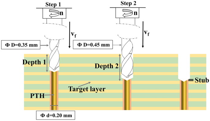
Start with thorough stackup analysis to identify vias needing backdrilling, focusing on those traversing unused inner layers. Specify backdrill depths in fabrication notes, accounting for drill breakout tolerances around 0.1 mm. Use verification holes at panel edges to confirm depth control, as per fabrication standards. Coordinate drill diameters: the backdrill bit exceeds the via drill by 0.1 to 0.2 mm to ensure stub clearance without damaging pads. Electric engineers should simulate post-backdrill S-parameters to validate improvements. Layer sequencing influences feasibility; symmetric stacks ease mechanical stability.
Fabrication partners require clear drill tables distinguishing primary and backdrill operations. Sequence backdrilling after plating to avoid residue issues. Inspect via integrity using cross-sectioning or electrical testing for opens or shorts. Combine backdrilling with via-in-pad or filled vias for ultimate optimization in dense designs. Avoid over-backdrilling, which risks weakening the board structure. These practices ensure reliable signal integrity backdrilling outcomes.
Related Reading: Backdrilling and Blind Vias: A Combined Approach to Signal Integrity
Cost considerations balance against performance gains; apply selectively to critical nets exceeding 3 Gbps. Collaborate early with manufacturers on capability matrices for depth accuracy. J-STD-001 supports assembly guidelines compatible with backdrilled boards. Test prototypes with TDR to measure stub remnants empirically. Iterate designs based on empirical data for successive builds. This methodical approach maximizes PCB performance optimization.
Troubleshooting Common Backdrilling Challenges
Engineers encounter depth variation leading to residual stubs or over-drills exposing inner traces. Mitigate by specifying tighter tolerances and using depth-controlled tooling. Plating voids in the transition zone signal inadequate cleanup; enhance with plasma desmear processes. Signal degradation persisting post-backdrilling often traces to antipad sizing; enlarge antipads to 1.5 times the backdrill diameter. Mechanical stress from asymmetric drilling warps thin cores; reinforce with sequential lamination. Cross-section analysis reveals most issues early.
Via resonance reappearing indicates incomplete stub removal; verify with X-ray or capacitance probing. Impedance mismatches arise from inconsistent dielectric around the barrel; uniform prepreg flow aids this. High-frequency PCB troubleshooting benefits from vector network analyzer sweeps pre- and post-fabrication. Document lessons in design rules for repeatability. These insights refine future iterations.
Conclusion
Backdrilling stands as a proven method for signal integrity backdrilling, directly tackling via resonance and impedance matching hurdles. High-frequency PCB designs achieve superior performance through this targeted optimization. Engineers gain confidence in scaling data rates without excessive redesigns. Integrating best practices ensures manufacturability and reliability. IPC standards like IPC-6012 and IPC-2221 guide these implementations effectively. Prioritizing backdrilling elevates overall PCB performance optimization.
FAQs
Q1: What is signal integrity backdrilling and when should engineers use it?
A1: Signal integrity backdrilling removes via stubs to prevent reflections in high-speed signals. Use it for nets above multi-Gbps rates where stub resonance impacts eye quality. It optimizes multilayer through-vias traversing unused layers. Combine with simulations for precise application. This technique enhances PCB performance optimization without blind vias.
Q2: How does backdrilling address via resonance in high-frequency PCBs?
A2: Backdrilling shortens stubs, shifting resonance frequencies beyond operational bands. This reduces S-parameter notches and improves insertion loss. Engineers model quarter-wavelength effects to justify depths. It maintains signal fidelity in dense routing. Essential for impedance matching continuity.
Q3: What are best practices for impedance matching with backdrilling?
A3: Specify backdrill diameters larger than via drills for annular gaps reducing capacitance. Verify depths with test holes per IPC guidelines. Simulate channel impedance pre-fabrication. Pair with ground vias for shielding. This ensures uniform 50/100-ohm profiles in high-frequency PCBs.
Q4: Can backdrilling impact PCB reliability negatively?
A4: Minimal if tolerances control depths accurately; over-drilling risks trace exposure. Proper sequencing post-plating preserves barrel integrity. Standards like IPC-6012 qualify such features. Inspect cross-sections routinely. Benefits outweigh risks for critical signals in performance-optimized boards.
References
IPC-6012E — Qualification and Performance Specification for Rigid Printed Boards. IPC, 2017
IPC-2221B — Generic Standard on Printed Board Design. IPC, 2012
IPC-4761 — Via Protection Guidelines. IPC, 2020
J-STD-001H — Requirements for Soldered Electrical and Electronic Assemblies. IPC, 2020