Introduction
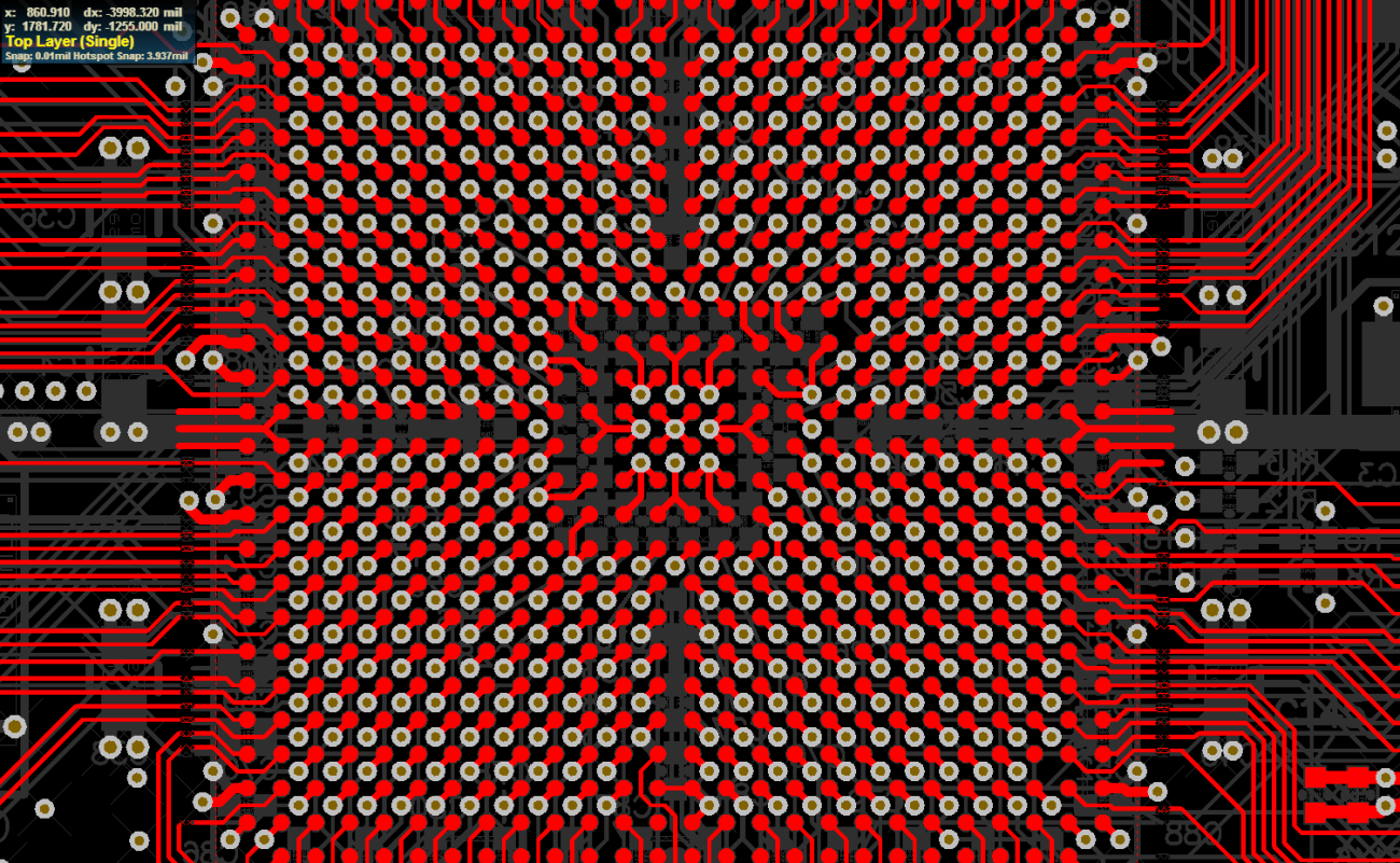
In modern PCB design, achieving optimal signal integrity becomes increasingly challenging as data rates climb into the gigahertz range. Electric engineers face the dilemma of balancing board density with high-frequency performance, particularly when routing signals from fine-pitch components like BGAs. Two prominent PCB routing techniques, via-in-pad and dog-bone routing, offer distinct approaches to fanout strategies. Via-in-pad signal integrity benefits from minimized trace lengths, while dog-bone routing provides a more conventional path for coarser pitches. This article delivers a structured comparison of these methods, focusing on their impact on signal integrity comparison and high-frequency performance. Understanding these PCB routing techniques equips designers to select the right strategy for demanding applications.
Understanding Dog-Bone Routing
Dog-bone routing involves placing a via slightly offset from the component pad and connecting them with a short trace, forming a shape resembling a dumbbell or dog bone. This technique allows the signal to transition from the surface pad to inner layers without overlapping the solder joint area. Engineers commonly apply it in designs with BGA pitches above 0.5 mm, where space permits the additional trace segment. The offset via prevents solder wicking into the hole during assembly, maintaining joint reliability. However, this extra trace introduces a small inductance loop, which can affect signal propagation in sensitive circuits. Overall, dog-bone routing remains a reliable choice for standard-density boards requiring straightforward fabrication.
Decoding Via-in-Pad Technology
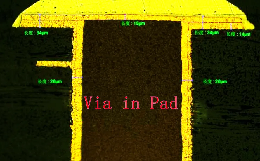
Via-in-pad places the via directly within the footprint of the component pad, eliminating the need for an interconnecting trace. Manufacturers typically fill the via with conductive or non-conductive epoxy and cap it with solder mask or plating to ensure planarity and prevent solder flow issues. This approach shines in high-density interconnects, enabling routing under the component for maximum space efficiency. Electric engineers favor it for BGAs with pitches below 0.5 mm, where traditional fanouts fail due to clearance constraints. The direct connection shortens the signal path, reducing parasitic effects that degrade performance. Proper implementation demands precise control over via dimensions and plating to meet quality standards.
Signal Integrity Fundamentals in High-Frequency PCBs
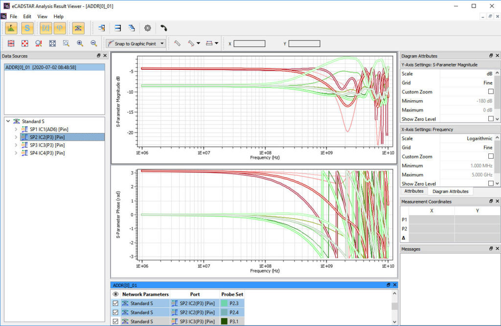
Signal integrity hinges on minimizing discontinuities like impedance mismatches and reflections caused by vias. In high-frequency performance scenarios, even short trace segments or via stubs can introduce unwanted resonances. Vias act as capacitive and inductive elements; the stub length beyond the signal layer creates a resonant frequency inversely proportional to its length. Backdrilling or using blind vias shortens stubs in both techniques, but the baseline path length differs significantly. Parasitic inductance from traces in dog-bone setups exacerbates return path disruptions, while via-in-pad maintains a straighter path to planes. Engineers must model these effects using field solvers to predict eye diagram quality and insertion loss.
Via-in-Pad Signal Integrity Advantages
Via-in-pad excels in via-in-pad signal integrity by eliminating the dog-bone trace, which typically adds 0.1 to 0.5 mm of extra length depending on layout. This reduction lowers loop inductance, preserving signal rise times and reducing crosstalk in dense routing. For signals above 5 GHz, the shorter path minimizes phase shifts and attenuation, critical for maintaining bit error rates below 10^-12. Filled vias also improve thermal dissipation by direct connection to inner planes, stabilizing temperatures during operation. Reliability aligns with IPC-6012E specifications for rigid boards, ensuring void-free fills and robust plating. In practice, this technique supports tighter impedance control, especially in controlled impedance stacks.
Dog-Bone Routing: Strengths and Limitations for SI
Dog-bone routing offers simplicity in fabrication, as it avoids the complexities of via filling and capping. The offset design facilitates easier inspection and reduces risks of solder entrapment, complying with IPC-A-600K acceptability criteria. However, the interconnect trace forms a small via fence effect, increasing inductance by up to 20% compared to direct connections in simulations. At high frequencies, this manifests as increased return loss, particularly if traces bend sharply. Engineers mitigate this by optimizing trace width and via size, but space constraints limit options in fine-pitch arrays. It suits applications where cost outweighs marginal SI gains, such as mid-range processors.
Head-to-Head Signal Integrity Comparison
- Signal Path Length — Via-in-Pad: Minimal (direct pad-to-via); Dog-Bone Routing: Extended by trace segment.
- Parasitic Inductance — Via-in-Pad: Lower due to no trace loop; Dog-Bone Routing: Higher from trace and offset.
- High-Frequency Performance — Via-in-Pad: Superior for >5 GHz (less reflection); Dog-Bone Routing: Adequate for <5 GHz.
- Density Enablement — Via-in-Pad: High (routing under BGA); Dog-Bone Routing: Moderate (requires fanout space).
- Fabrication Complexity — Via-in-Pad: Higher (fill, cap, planarize); Dog-Bone Routing: Lower (standard via process).
- Cost — Via-in-Pad: Elevated for HDI boards; Dog-Bone Routing: Economical for standard builds.
This list highlights key trade-offs in signal integrity comparison. Via-in-pad dominates in high-frequency performance metrics like insertion loss, while dog-bone provides a cost-effective baseline. Selection depends on pitch, layer count, and speed requirements. Simulations confirm via-in-pad reduces near-end crosstalk by optimizing field distribution.
Best Practices for PCB Routing Techniques
Start by assessing BGA pitch: opt for dog-bone above 0.65 mm and via-in-pad below. Always incorporate backdrilling for through vias to stub lengths under 0.5 mm, preserving high-frequency performance. Maintain annular ring widths per IPC-2221 guidelines to prevent breakout failures. For via-in-pad, specify non-conductive fill for signal vias to avoid shorts, and conductive for power. Simulate SI early, targeting 100-ohm differential impedance with <5% variation. Test prototypes with TDR to validate models, adjusting as needed.
Implementation Considerations and Troubleshooting
In multilayer boards, via-in-pad facilitates any-layer vias in HDI stacks, unlocking routing density. Common pitfalls include tenting failures leading to solder voids; mitigate with precise mask registration. Dog-bone traces demand stub staggering to avoid resonance alignment across channels. Thermal cycling stresses filled vias, so validate per JEDEC J-STD-020E for reflow sensitivity. Troubleshooting reflections often traces to unbackdrilled stubs; oscilloscope captures reveal them as post-cursor ISI. Logical iteration between design, fab, and test ensures robust outcomes.
Conclusion
Via-in-pad and dog-bone routing represent pivotal PCB routing techniques tailored to density and speed needs. Via-in-pad signal integrity outperforms in high-frequency performance through path minimization, ideal for cutting-edge designs. Dog-bone routing delivers reliable, economical solutions for less demanding pitches. Engineers benefit from structured evaluation of trade-offs, backed by simulation and standards compliance. Selecting the optimal method enhances overall board reliability and performance margins.
FAQs
Q1: What improves high-frequency performance more: via-in-pad or dog-bone routing?
A1: Via-in-pad generally provides better high-frequency performance by eliminating the trace segment in dog-bone setups, reducing inductance and reflections. This shortens the signal path, preserving eye opening at multi-GHz rates. Logical SI analysis confirms lower insertion loss, though backdrilling applies to both for stub control. Fabrication readiness influences final choice.
Q2: When should electric engineers choose via-in-pad for signal integrity?
A2: Opt for via-in-pad in fine-pitch BGAs under 0.5 mm pitch or high-density routing where fanout space is limited. It enhances via-in-pad signal integrity by direct connectivity, minimizing parasitics. Ensure fab capabilities support filling and capping per standards. This technique suits RF and high-speed digital boards.
Q3: How does dog-bone routing impact signal integrity comparison?
A3: Dog-bone routing introduces modest inductance from the offset trace, slightly degrading signal integrity compared to via-in-pad at high speeds. It excels in manufacturability for coarser pitches, with easier assembly inspection. Mitigate effects via short traces and impedance tuning. Suitable for cost-sensitive mid-range designs.
Q4: What PCB routing techniques align with IPC standards for vias?
A4: Both via-in-pad and dog-bone must adhere to IPC guidelines like IPC-6012E for via quality and annular rings. Proper plating and fill prevent reliability issues. Signal integrity comparison favors optimized implementations. Consult specs during design for compliance.
References
IPC-6012E — Qualification and Performance Specification for Rigid Printed Boards. IPC, 2015
IPC-A-600K — Acceptability of Printed Boards. IPC, 2020
IPC-2221B — Generic Standard on Printed Board Design. IPC, 2012
JEDEC J-STD-020E — Moisture/Reflow Sensitivity Classification. JEDEC, 2014


