Introduction
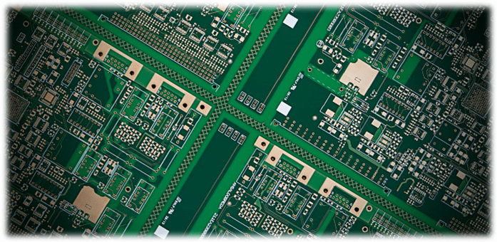
High-density printed circuit boards pack thousands of components into minimal footprints, driving innovations in electronics like smartphones and medical devices. In these compact spaces, silkscreen markings serve as the visual roadmap for assembly, testing, and repair processes. However, achieving silkscreen legibility in tight spaces becomes a critical engineering challenge as component pitches shrink below 0.5 mm. Poorly designed silkscreen can lead to assembly errors, increased rework time, and reliability issues down the line. This article explores PCB silkscreen design for small components, offering logical strategies to maintain clarity amid high-density PCB marking constraints. Electrical engineers will find structured insights into balancing space efficiency with readability.
What Is PCB Silkscreen and Why It Matters in High-Density Designs
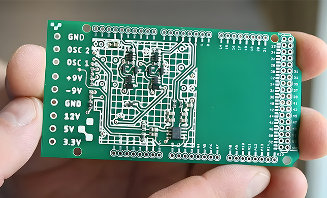
PCB silkscreen, also known as the legend or nomenclature layer, consists of printed ink applied to the board surface to convey essential information. This layer includes reference designators, polarity indicators, part numbers, and assembly notes, all rendered in white or contrasting colors over the solder mask. In standard boards, silkscreen poses few issues, but high-density designs amplify its importance due to component identification challenges. Clear markings directly impact surface-mount technology assembly accuracy, where automated pick-and-place machines and human inspectors rely on precise labels. Without legible silkscreen, troubleshooting faults in multilayer stacks becomes inefficient, potentially delaying production cycles.
The relevance escalates in high-density interconnect boards, where fine-pitch BGAs and 01005 passives leave scant room for text. Industry standards like IPC-A-600 outline acceptability criteria for markings, ensuring they withstand fabrication stresses such as reflow soldering. Engineers must prioritize silkscreen from the schematic capture stage, integrating it seamlessly with layout constraints. Ultimately, effective high-density PCB marking enhances yield rates and supports long-term board maintainability.
Key Challenges in Silkscreen Legibility for Tight Spaces
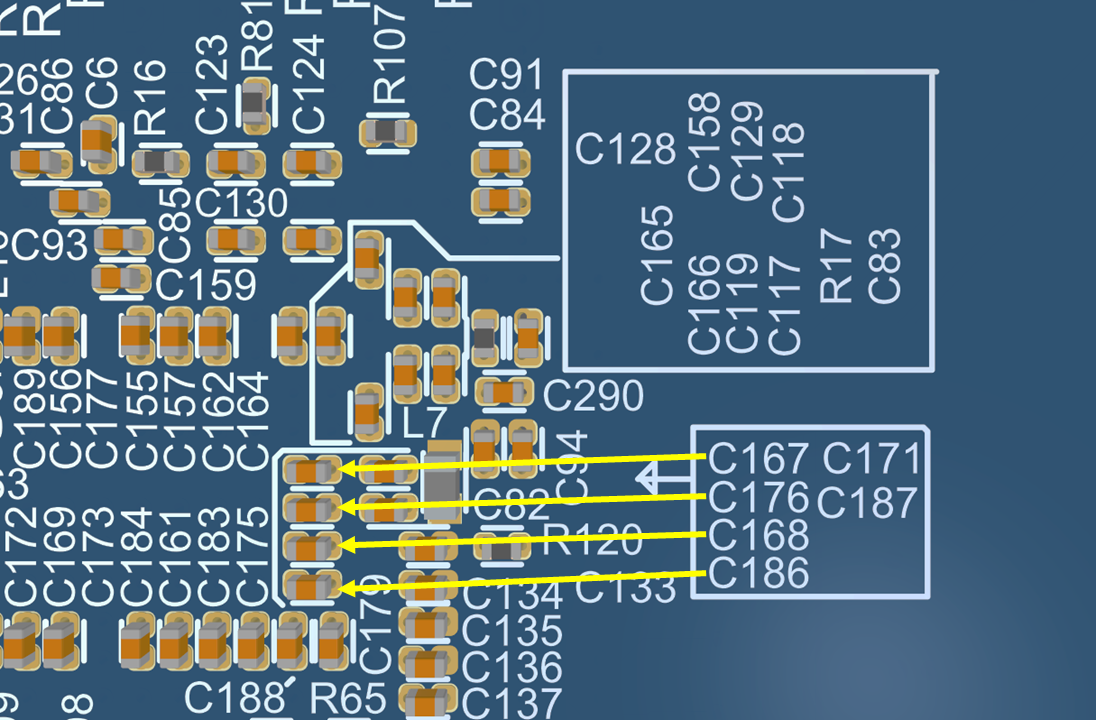
Component identification challenges arise primarily from spatial limitations in high-density layouts. Tiny components like 0201 resistors or 0.3 mm pitch QFNs crowd the board, squeezing silkscreen elements into sub-millimeter gaps. Overlapping labels or proximity to pads risks ink bleed during printing, rendering text unreadable under inspection lights. Additionally, varying board finishes, such as ENIG or OSP, affect ink adhesion and contrast, complicating legibility across production runs.
Miniaturized silkscreen fonts exacerbate these issues, as thinner strokes blur at the limits of printing resolution. Fabrication processes struggle with features below certain thresholds, leading to filled-in characters or halos around edges. Thermal cycling during assembly can further degrade markings if ink durability falters. Engineers face a trade-off: maximizing information density without sacrificing post-reflow clarity. These factors underscore the need for proactive design rules tailored to high-density environments.
Technical Principles Governing Silkscreen Performance
Silkscreen legibility hinges on the interplay of ink application methods, material properties, and geometric design. Traditional screen printing uses stencils with emulsions, limiting resolution to around 0.15 mm line widths due to ink viscosity and mesh tension. Liquid photoimageable (LPI) silkscreen, preferred for high-density boards, employs UV-curable inks exposed through photomasks, achieving finer details akin to solder mask processes. This shift enables miniaturized silkscreen fonts while maintaining edge definition.
Contrast plays a pivotal role, with white ink over green solder mask providing optimal visibility, though black or yellow suits dark masks. Font geometry influences readability: sans-serif styles with uniform stroke widths resist distortion better than serifs. IPC-7351 guidelines for component footprints specify silkscreen placement for polarity and pin-1 indicators, ensuring standardized visibility regardless of density. Substrate warpage or copper topography can distort prints, so flatness control during lamination proves essential.
Resolution limits tie directly to aspect ratios in artwork generation. High line-to-space ratios prevent bridging, while positive versus negative imaging affects fill consistency. Environmental factors, including humidity during curing, impact ink polymerization. Understanding these mechanisms allows engineers to predict and mitigate defects in compact designs.
Best Practices for High-Density PCB Silkscreen Design
Start with font selection optimized for PCB silkscreen design for small components. Choose vector-based, monospaced fonts like those with 1:6 height-to-stroke ratios to ensure scalability without pixelation. Avoid cursive or overly decorative styles that compromise machine readability. Position reference designators immediately adjacent to component outlines, ideally outside the courtyard to evade solder paste interference.
Maintain clearances: at least 0.1 mm from pads, vias, and traces to prevent shorts or ink encroachment. Orient all text horizontally for uniform scanning, rotating only symbols if space demands. In ultra-tight areas, employ abbreviations (e.g., "R" for resistor) or icons for capacitors and diodes, reducing footprint while preserving meaning. Leverage both top and bottom layers for distributed marking, cross-referencing via fiducials.
For high-density PCB marking, validate designs through design rule checks (DRC) enforcing minimum feature sizes. Simulate printing with Gerber viewers to spot overlaps early. Select matte inks for glare reduction under LED inspection. IPC-6012 performance specifications guide qualification, verifying markings endure thermal and mechanical stresses.
Layer stacking order matters: apply silkscreen post-solder mask to avoid mask bleed-over. Test prototypes under microscope for legibility at 10x magnification, simulating assembly conditions. These practices systematically address silkscreen legibility in tight spaces.
Troubleshooting Common Silkscreen Issues in Compact Boards
Misalignment often stems from artwork scaling errors or panelization offsets, verifiable via automated optical inspection (AOI). If characters appear filled, upscale strokes or switch to LPI processes for better resolution. Smudging indicates excessive ink thickness; adjust squeegee pressure in fabrication dialogues.
Fading post-reflow points to ink incompatibility with flux residues, resolved by high-temperature formulations. In high-density scenarios, partial clipping occurs from overcrowding; depopulate non-essential labels or use QR codes for supplementary data. Cross-section analysis reveals adhesion failures, linking back to surface preparation.
Document deviations in assembly drawings when silkscreen yields to density imperatives. Periodic audits against IPC-A-600 criteria maintain compliance. Logical root-cause analysis streamlines resolutions, minimizing iterations.
Advanced Insights: Integrating Silkscreen with HDI Features
High-density interconnect (HDI) boards introduce microvias and blind/buried layers, further compressing surface real estate. Route silkscreen around via farms, using stacked vias' exposed annuli as natural guides. For fan-out zones under BGAs, cluster labels radially to exploit symmetry.
Hybrid marking combines silkscreen with laser-etched codes for traceability, though silkscreen remains primary for ref des. Finite element modeling predicts warpage effects on print fidelity, informing stackup choices. These integrations elevate component identification challenges into managed variables.
Conclusion
Mastering silkscreen design in high-density PCBs demands a structured approach to overcome spatial constraints. By adhering to principles of resolution, contrast, and placement, engineers achieve reliable legibility for small components. Best practices like strategic abbreviations and DRC enforcement mitigate common pitfalls, aligning with standards such as IPC-7351 and IPC-6012. Ultimately, thoughtful high-density PCB marking not only boosts assembly efficiency but also fortifies product longevity. Prioritize these strategies in your next layout to navigate miniaturized silkscreen fonts effectively.
FAQs
Q1: What are the main component identification challenges in high-density PCB marking?
A1: In high-density designs, tiny pitches between components like QFNs and passives limit space for labels, risking overlaps and ink bleed. Fabrication resolution caps feature sizes, blurring miniaturized silkscreen fonts during printing or reflow. Strategic placement and abbreviations address these, ensuring readability for assembly and rework. Standards like IPC-A-600 define acceptability to guide compliance.
Q2: How can engineers improve silkscreen legibility in tight spaces?
A2: Prioritize sans-serif fonts with adequate stroke widths and horizontal orientation for uniform visibility. Maintain clearances from pads and vias, distributing labels across layers if needed. LPI processes enhance resolution over traditional screening. Validate via prototypes under magnification to confirm post-process clarity.
Q3: What role does IPC-7351 play in PCB silkscreen design for small components?
A3: IPC-7351 standardizes footprint silkscreen for polarity and pin-1 indicators, critical in dense layouts. It ensures consistent placement relative to lands, aiding automated assembly. Designers reference it to avoid custom deviations that compromise legibility.
Q4: Why is font choice crucial for miniaturized silkscreen fonts on high-density boards?
A4: Monospaced, uniform-stroke fonts scale reliably without distortion at fine resolutions. They resist fill-in from ink spread, maintaining contrast post-fabrication. Poor choices amplify legibility issues in compact spaces, increasing error risks during inspection.
References
IPC-A-600K — Acceptability of Printed Boards. IPC, 2020
IPC-7351C — Generic Requirements for Surface Mount Design and Land Pattern Standard. IPC, 2010
IPC-6012E — Qualification and Performance Specification for Rigid Printed Boards. IPC, 2017


