Introduction
Silkscreen on printed circuit boards serves as the essential labeling layer that guides assembly processes, identifies components, and supports troubleshooting during production and maintenance. This non-conductive ink layer includes reference designators, polarity indicators, part numbers, and other critical markings that technicians rely on for accurate component placement and verification. However, PCB silkscreen errors can lead to significant assembly delays, rework costs, and even functional failures if not addressed early in the design phase. Common issues like silkscreen over pads, silkscreen over vias, and silkscreen misplacement often arise from overlooked design rules, compromising solder joint quality and overall board reliability. For electrical engineers focused on PCB assembly, understanding these silkscreen design flaws is crucial to streamline manufacturing and minimize defects. By avoiding silkscreen readability issues and other pitfalls, designs achieve smoother transitions from fabrication to assembly lines.
What Is PCB Silkscreen and Why It Matters in Assembly
PCB silkscreen, also known as the legend or markup layer, consists of printed epoxy-based ink applied to the board's surface, typically on top of the solder mask. It provides visual cues such as component outlines, pin-1 indicators, and test point labels that are vital for manual and automated assembly operations. During surface-mount technology processes, operators and pick-and-place machines use these markings to ensure precise component orientation and placement. In high-volume assembly, clear silkscreen reduces inspection time and error rates, directly impacting yield and throughput. Poor silkscreen quality can obscure these references, leading to misaligned parts, polarity reversals, or incorrect soldering, which cascade into electrical failures post-assembly. Adhering to established guidelines ensures silkscreen supports the entire assembly workflow, from stencil printing to final functional testing.
Common Causes of PCB Silkscreen Errors
Silkscreen design flaws often stem from insufficient design rule checks or ignoring manufacturing tolerances during layout. Registration inaccuracies between layers can shift markings relative to pads and vias, exacerbating issues in dense boards. Ink application processes, involving screen printing or direct legend printing, amplify flaws if designs push process limits. Electrical engineers must consider these mechanisms to prevent propagation into assembly stages. Overly ambitious layouts prioritizing space over clarity frequently introduce silkscreen misplacement and readability problems. Proactive DRC implementation catches many of these early.
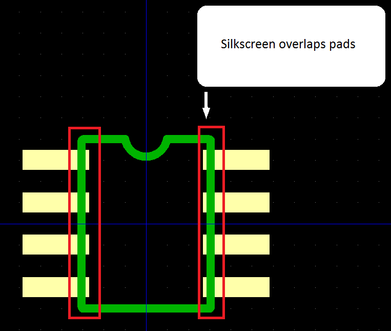
Silkscreen Over Pads: A Critical Assembly Risk
One of the most prevalent PCB silkscreen errors is placing legend ink directly over solder pads, which interferes with wetting during reflow soldering. The non-conductive ink residue prevents molten solder from forming reliable joints, resulting in cold solder defects or open circuits detectable only after assembly. Fabricators typically clip or remove such silkscreen during processing to comply with acceptability criteria, but this leaves incomplete labels that confuse assemblers. According to IPC-A-600 guidelines on printed board acceptability, markings over solderable surfaces are considered nonconforming and must be avoided to maintain joint integrity. In troubleshooting, engineers observe de-wetting or bridging around affected pads during visual inspection or X-ray analysis. To mitigate, always enforce clearance rules in PCB software that prohibit silkscreen overlap with pad openings.
Silkscreen Over Vias: Hidden Contamination Hazards
Silkscreen over vias introduces another serious design flaw, as ink can seep into open via holes during printing, potentially causing shorts or blocking plating processes. Untented vias are particularly vulnerable, with excess ink leading to reliability issues under thermal cycling in assembly reflow. This error often goes unnoticed until electrical testing reveals intermittent connections or increased resistance. Assembly teams report higher failure rates in boards with such flaws, complicating root cause analysis. Best practice involves routing silkscreen to skirt via peripheries, ensuring no overlap even with alignment tolerances. Regular Gerber reviews confirm compliance before fabrication.
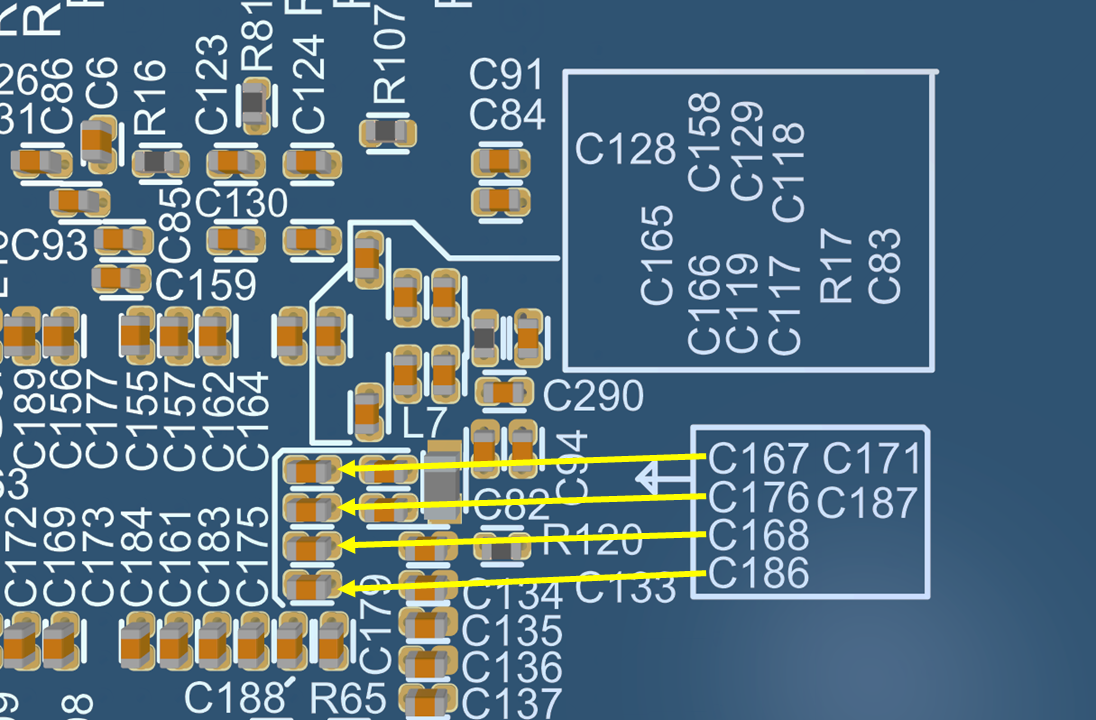
Silkscreen Misplacement: Alignment and Tolerance Challenges
Silkscreen misplacement occurs when labels stray too close to features or shift due to layer registration errors, disrupting assembly workflows. Tolerances in printing equipment, typically in the range of fabrication capabilities, demand buffer zones around pads and components. Misaligned reference designators force operators to hunt for matches, slowing hand assembly and increasing placement errors in automated lines. This flaw compounds in multi-layer boards where fiducials fail to compensate fully. Engineers troubleshoot by overlaying Gerber layers in viewers to simulate misalignments. Consistent fiducial placement and conservative spacing resolve most cases.
Silkscreen Readability Issues: Visibility Under Stress
Silkscreen readability issues arise from thin strokes, inadequate contrast, or fonts prone to bleeding during ink curing. Faint or distorted text becomes illegible under factory lighting or after reflow exposure, hindering component verification. Crowded layouts exacerbate this, merging characters and obscuring polarity marks essential for diode and capacitor placement. Per IPC-4781 specifications for legend inks, materials must withstand assembly environments without fading or cracking. Troubleshooting involves magnification checks and contrast simulations in design tools. Selecting bold, sans-serif styles and high-contrast colors like white on green solder mask prevents these problems.
Additional Silkscreen Design Flaws to Watch
Beyond primary errors, inconsistent text orientation across the board complicates 180-degree flips during assembly, leading to repeated handling mistakes. Omitting critical elements like assembly notes or date codes hampers traceability in production runs. Overloading the layer with non-essential graphics reduces space for vital labels, inviting omissions. Vias and fiducials under silkscreen also risk obscuration, affecting alignment jigs. Electrical engineers prioritize functional markings first, culling extras via iterative reviews.
Best Practices for Flawless Silkscreen Design
Implement design rule checks prohibiting silkscreen over pads and vias, with clearances accounting for process tolerances. Position reference designators adjacent to components for quick association, using simple vector fonts for sharpness. Ensure uniform readability by aligning all text horizontally and selecting inks compliant with IPC-4781 for durability through reflow and cleaning. Review bottom-side silkscreen equally, as it aids wave soldering and inspection. Prototype testing validates legibility under simulated assembly conditions. Collaborate with fabricators on DFM feedback to refine rules iteratively.
Troubleshooting Silkscreen Issues During PCB Assembly
In assembly, spot silkscreen errors via incoming inspection, comparing Gerbers to bare boards for clipping or shifts. Use AOI systems programmed for legend presence and clarity on high-volume lines. For misplacement, adjust pick-and-place offsets based on fiducials, but redesign prevents recurrence. Readability failures trigger manual verification stations, bottlenecking flow. Post-reflow, check for ink migration affecting joints with cross-sectioning if needed. Document flaws in yield reports to feedback design teams promptly.
Conclusion
Avoiding PCB silkscreen errors demands vigilance in design, from clearances around pads and vias to ensuring robust readability. These practices safeguard assembly efficiency, reducing defects and rework. Electrical engineers benefit from standards like IPC-A-600 and IPC-4781 to align designs with manufacturing realities. Integrating DFM early yields error-free boards ready for demanding applications. Prioritize silkscreen as a functional layer, not decorative, for optimal outcomes.
FAQs
Q1: What are the most common PCB silkscreen errors impacting assembly?
A1: PCB silkscreen errors like silkscreen over pads, silkscreen over vias, and silkscreen misplacement top the list, as they disrupt soldering and component placement. Readability issues from thin fonts or poor contrast further complicate operator verification. Troubleshooting focuses on Gerber reviews and DFM checks to catch these pre-production. Adhering to IPC guidelines minimizes risks effectively.
Q2: How does silkscreen over pads cause assembly failures?
A2: Silkscreen over pads deposits ink that inhibits solder wetting, leading to weak joints or opens during reflow. Fabricators clip the ink per acceptability standards, but residual misalignment persists. Assembly yields drop as technicians misidentify sites. Prevent by enforcing no-overlap rules in layout software and verifying clearances.
Q3: What steps prevent silkscreen readability issues?
A3: To avoid silkscreen readability issues, use bold fonts with sufficient stroke width, high-contrast colors, and consistent orientation. Space elements to prevent crowding and simulate printing tolerances. Test prototypes under assembly lighting. IPC-4781 ensures ink withstands processes without degradation.
Q4: Can silkscreen over vias be tolerated in designs?
A4: Silkscreen over vias risks ink contamination in open holes, causing shorts or blocks post-assembly. Even tented vias warrant caution due to potential cracking. Always offset markings and run DRCs. This flaw elevates test failures unnecessarily.
References
IPC-A-600K — Acceptability of Printed Boards. IPC, 2020
IPC-4781 — Qualification and Performance Specification of Permanent, Semi-Permanent and Temporary Legend and/or Marking Inks. IPC, 2008
IPC-6012E — Qualification and Performance Specification for Rigid Printed Boards. IPC, 2017


