Introduction
In the realm of printed circuit board (PCB) design, selecting the right component mounting technology is a critical decision that impacts performance, manufacturability, and cost. Surface Mount Device (SMD) and Through-Hole Technology (THT) represent two fundamental approaches, each with distinct footprint designs that influence PCB layout and assembly. For electrical engineers, understanding the nuances of SMD footprint design and through-hole footprint design is essential for achieving PCB design optimization. This article explores the differences between these technologies through a detailed component footprint comparison. It examines their technical characteristics, design considerations, and best practices for optimizing layouts. By aligning with industry standards and focusing on practical applications, this discussion aims to equip engineers with the knowledge needed to make informed decisions for their projects.
What Are SMD and Through-Hole Technologies?
SMD and Through-Hole are two primary methods for mounting electronic components onto PCBs. SMD components are soldered directly onto the surface of the board using pads, enabling compact designs suitable for high-density layouts. Through-Hole components, on the other hand, have leads that pass through drilled holes in the PCB and are soldered on the opposite side, offering robust mechanical strength. The choice between these technologies affects not only the footprint design but also the overall performance and reliability of the circuit. In modern electronics, where space constraints and production efficiency are paramount, understanding the implications of each method through component footprint comparison is vital for PCB design optimization. Both approaches have unique advantages, making them relevant across various applications, from consumer gadgets to industrial systems.
Technical Principles of Footprint Design
SMD Footprint Design
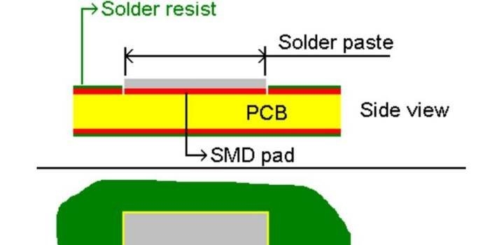
SMD footprint design focuses on creating precise land patterns on the PCB surface to accommodate components without through-holes. These patterns consist of solder pads that match the component's terminals, ensuring proper alignment during PCB assembly. The design must account for pad size, shape, and spacing to facilitate soldering and prevent defects like tombstoning or bridging. Industry standards, such as IPC-7351B, provide guidelines for optimal pad dimensions and tolerances for surface mount components. These standards help engineers achieve reliable solder joints while maximizing board space. SMD designs are ideal for automated assembly processes due to their compatibility with pick-and-place machines, but they require careful attention to thermal management and solder paste application.
Through-Hole Footprint Design
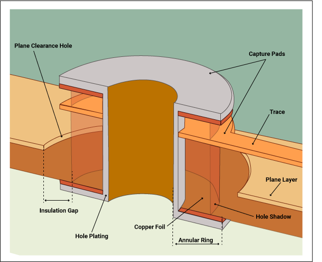
Through-hole footprint design involves creating holes in the PCB for component leads, with annular rings around each hole to provide a soldering area. The design must ensure adequate hole diameter and pad size to accommodate the lead and allow for proper solder flow. Standards like IPC-2221B offer specifications for hole spacing, pad dimensions, and clearance to ensure durability and ease of assembly. Through-hole components provide strong mechanical bonding, making them suitable for applications subject to vibration or stress. However, they occupy more board space and are less suited for high-density designs compared to SMD. The drilling process also adds to manufacturing complexity and PCB cost.
Component Footprint Comparison
A direct component footprint comparison reveals key differences between SMD and Through-Hole designs. SMD footprints are smaller, allowing for tighter component placement and reduced board size, which is critical for PCB design optimization in compact devices. Through-hole footprints, due to the need for holes and larger pads, require more space and often limit component density. SMD designs support finer pitch components, enabling advanced miniaturization, while through-hole designs are constrained by drilling tolerances. Additionally, SMD soldering occurs on one side of the board, simplifying multilayer designs, whereas through-hole soldering may involve both sides, impacting routing complexity. Engineers must weigh these factors based on project requirements like space, cost, and mechanical needs.
- Board Space: SMD—Compact, high-density layouts; Through-Hole—Larger footprint, less density.
- Assembly Method: SMD—Surface soldering, automated; Through-Hole—Lead insertion, manual or wave soldering.
- Mechanical Strength: SMD—Moderate, relies on solder joint; Through-Hole—High, robust lead bonding.
- Design Complexity: SMD—Precise pad alignment needed; Through-Hole—Hole drilling and spacing critical.
Practical Solutions for PCB Design Optimization
Optimizing SMD Footprint Design
To achieve PCB design optimization with SMD components, engineers should adhere to standardized guidelines for pad design. Following IPC-7351B ensures that pad sizes and spacing match component specifications, reducing the risk of soldering defects. Proper SMT stencil design for solder paste application is also crucial to avoid excess or insufficient paste. Thermal considerations are important, as SMD components are sensitive to heat during reflow soldering. Providing thermal reliefs or vias near power components can help dissipate heat effectively. Additionally, maintaining clearance between components prevents interference during assembly and allows for rework if needed. Testing the layout with design rule checks (DRC) ensures compliance with manufacturing capabilities.
Optimizing Through-Hole Footprint Design
For through-hole footprint design, optimization begins with selecting appropriate hole sizes and pad dimensions as per IPC-2221B standards. Ensuring sufficient annular ring width around holes supports strong solder joints and prevents breakout during drilling. Spacing between holes must account for mechanical stress and ease of insertion, especially for manual assembly. Using plated-through holes can enhance electrical conductivity and structural integrity in multilayer boards. Engineers should also consider the impact of through-hole components on routing, as leads can obstruct inner layers. Balancing component placement to minimize board warpage during soldering is another key factor for reliability.
Balancing SMD and Through-Hole in Hybrid Designs
Many modern PCBs combine SMD and Through-Hole components to leverage the strengths of both. In such hybrid designs, PCB design optimization requires careful planning of component placement and routing. Place SMD components on one side for automated assembly, while reserving through-hole components for areas needing mechanical strength. Ensure that through-hole drilling does not interfere with SMD pad layouts or signal traces. Standards like IPC-A-600K can guide acceptable board fabrication practices to maintain quality. Hybrid designs often demand iterative testing to refine footprint layouts and ensure compatibility with assembly processes.
Troubleshooting Common Footprint Design Challenges
Footprint design errors can lead to assembly failures or reduced board reliability. For SMD footprint design, insufficient pad spacing may cause solder bridging, where adjacent pads connect unintentionally. Adjusting pad dimensions and using solder mask layers as per IPC-7351B can mitigate this issue. In through-hole footprint design, undersized holes can hinder lead insertion, while oversized holes weaken solder joints. Adhering to IPC-2221B for hole tolerances resolves such problems. Thermal mismatch between components and the board during soldering is another concern for both technologies. Incorporating thermal vias or adjusting reflow profiles based on industry guidelines helps manage heat distribution. Regular design reviews and simulations are recommended to identify potential issues before fabrication.
Conclusion
Selecting between SMD and Through-Hole technologies for PCB design involves a thorough understanding of footprint design principles and their impact on performance. SMD footprint design excels in high-density applications, offering space efficiency and compatibility with automated assembly. Through-hole footprint design provides unmatched mechanical strength, ideal for rugged environments. Through a detailed component footprint comparison, engineers can identify the best approach for their specific needs. By following established standards like IPC-7351B and IPC-2221B, and applying best practices for PCB design optimization, reliable and efficient layouts are achievable. Balancing technical requirements with manufacturing constraints ensures that the chosen design meets both functional and economic goals.
FAQs
Q1: What are the key differences in SMD footprint design compared to through-hole footprint design?
A1: SMD footprint design focuses on surface pads for compact, high-density layouts, guided by standards like IPC-7351B for precise alignment and soldering. Through-hole footprint design requires drilled holes and larger pads, following IPC-2221B, prioritizing mechanical strength over space efficiency. SMD suits automated assembly, while through-hole supports robust bonding for demanding applications.
Q2: How does component footprint comparison impact PCB design optimization?
A2: Component footprint comparison reveals trade-offs between space, strength, and assembly methods. SMD footprints enable smaller, denser designs, optimizing board real estate. Through-hole footprints offer durability but consume more space. Understanding these differences allows engineers to align designs with project goals, balancing cost, performance, and manufacturability for effective PCB design optimization.
Q3: What standards should guide SMD footprint design for reliable assembly?
A3: IPC-7351B is the primary standard for SMD footprint design, specifying pad size, shape, and tolerance for surface mount components. It ensures compatibility with automated assembly and minimizes soldering defects. Following these guidelines helps achieve consistent, high-quality solder joints and supports overall board reliability during production.
Q4: Why is through-hole footprint design still relevant in modern PCB layouts?
A4: Through-hole footprint design remains relevant for applications requiring high mechanical strength, such as industrial or automotive systems. Guided by IPC-2221B, it ensures robust lead bonding under stress or vibration. Despite larger space requirements, it is often used in hybrid designs alongside SMD for critical components needing durability.
References
IPC-7351B — Generic Requirements for Surface Mount Design and Land Pattern Standard. IPC, 2010.
IPC-2221B — Generic Standard on Printed Board Design. IPC, 2012.
IPC-A-600K — Acceptability of Printed Boards. IPC, 2020.


