Introduction
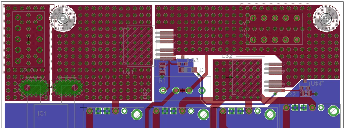
Power electronics applications, such as motor drives, power supplies, and inverters, demand PCBs capable of handling substantial currents while maintaining reliability and efficiency. High current PCB design requires careful attention to power distribution to prevent overheating, voltage drops, and failures under load. Engineers face challenges like excessive resistance in traces, poor heat dissipation, and electromagnetic interference when currents exceed standard levels. Advanced techniques focus on optimizing conductor sizing, thermal pathways, and layout strategies to ensure stable performance. This article explores proven methods to tame high currents, drawing on established engineering principles for robust designs.
Why High Current PCB Design Matters in Power Electronics
High current PCB design is essential for applications where power levels push beyond conventional signal processing boards. In power electronics, currents can reach tens or hundreds of amperes, leading to significant I2R losses if not managed properly. Poor power distribution results in hotspots, reduced component lifespan, and system inefficiencies. According to IPC-2152 standards, accurate determination of current carrying capacity prevents thermal runaway and ensures board integrity. Designers must prioritize these aspects to meet performance specs in demanding environments like renewable energy systems and electric vehicles. Ultimately, effective high current strategies enhance overall system reliability and cost-effectiveness.
Core Principles of Power Distribution in High Current PCBs
Power distribution in high current PCBs relies on minimizing resistance and managing generated heat through strategic conductor geometry. Wide traces and solid power planes reduce voltage drops across the board. Copper thickness, often expressed as weight per square foot, directly influences current handling; heavier copper layers offer lower resistance paths for sustained high loads. Thermal principles play a critical role, as Joule heating from current flow must dissipate without exceeding material limits. Engineers evaluate these factors during layout to balance electrical and thermal performance. Structured analysis of cross-sectional area and ambient conditions guides optimal configurations.
Understanding Current Carrying Capacity
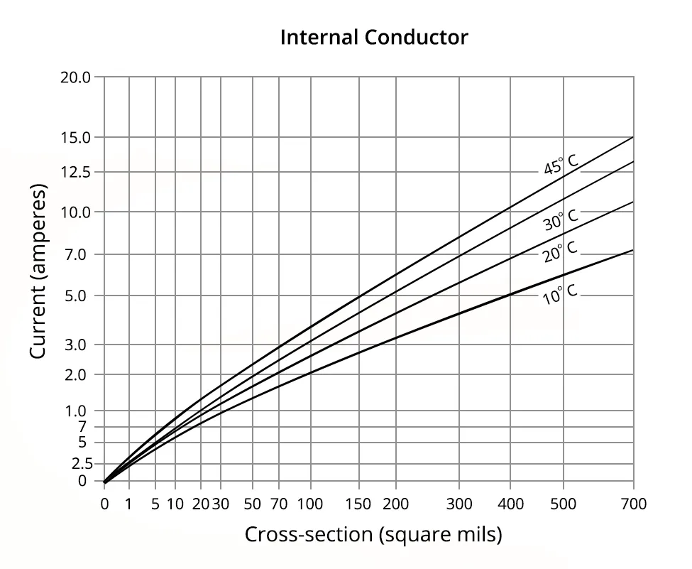
Current carrying capacity defines the maximum current a conductor can handle without excessive temperature rise. Factors like trace width, thickness, board layers, and airflow affect this metric. IPC-2152 provides comprehensive charts accounting for internal versus external traces and varying copper cross-sections. Designers use these to select dimensions that keep temperature rises within safe margins, typically targeting 10-20°C above ambient depending on application. Surrounding copper planes also influence capacity by aiding heat spreading. Proper assessment avoids undersized conductors that lead to premature failures.
Optimizing Power Plane Copper Weight
Power plane copper weight is a cornerstone of high current PCB design, with standard 1 oz/ft2 escalating to 2 oz, 3 oz, or more for heavy-duty needs. Thicker copper lowers sheet resistance, enabling broader current distribution without localized heating. However, heavier planes demand adjusted etching processes and increase board weight and cost. In multilayer boards, dedicating inner layers to power planes maximizes area utilization while shielding signal lines. Engineers calculate effective resistance using plane dimensions and verify against load requirements. This approach ensures uniform voltage delivery to power components.
Leveraging Thermal Vias for Enhanced Heat Dissipation
Thermal vias serve as vertical conduits for heat transfer from surface components to inner planes or the opposite side. Arrays of plated vias under hot spots, like power MOSFETs, create low-thermal-resistance paths. Via diameter, pitch, and filling options impact performance; smaller diameters allow denser packing but may restrict heat flow if not optimized. Connecting vias to large copper pours spreads heat laterally for better dissipation. In high current designs, thermal vias complement natural convection and forced air cooling. Consistent implementation prevents thermal bottlenecks in dense layouts.
Strategic Power MOSFET Layout Techniques
Power MOSFET layout demands proximity between source, drain, and gate to minimize parasitic inductances that cause voltage spikes during switching. Placing MOSFETs on dedicated power islands with short, wide connections to planes reduces loop areas. Kelvin sensing for gate drive signals improves accuracy amid high currents. Symmetrical arrangements for paralleled devices balance current sharing and heat generation. Adjacent decoupling capacitors stabilize supply rails against transients. These layout choices align with IPC-2221 guidelines for conductor spacing and thermal relief, ensuring stable operation at high frequencies.
Advanced Heat Dissipation Strategies
Heat dissipation in high current PCBs integrates multiple techniques beyond basic vias. Embedded copper coins or heat slugs under critical components conduct heat to external sinks. Via tents or fills prevent solder wicking while maintaining paths. Multilayer stackups with dedicated thermal planes sandwich components for three-dimensional spreading. Surface treatments like thermal pads interface with heatsinks effectively. Simulation tools verify junction temperatures against datasheet limits pre-fabrication. Layered approaches yield superior performance in compact power electronics modules.
Best Practices for Implementation
Start with stackup planning to allocate thick copper for power layers adjacent to ground for impedance control. Simulate current density and thermal profiles early to iterate designs. Use stitching vias along plane edges to equalize potentials and enhance structural integrity. For power MOSFETs, prioritize short high-current paths and isolate control signals. Validate prototypes with thermal imaging under full load. Document deviations from standards with justifications for team review. These practices yield reliable high current PCB designs ready for production.
Conclusion
Mastering high current PCB design involves integrating robust power planes, precise current carrying capacity calculations, and effective thermal management. Techniques like increased power plane copper weight, thermal vias, and optimized power MOSFET layouts directly address the demands of power electronics. By adhering to principles from IPC standards, engineers achieve designs that deliver high performance without compromise. Prioritizing these strategies minimizes risks and extends system life. Future advancements will build on these foundations for even higher power densities.
FAQs
Q1: What factors determine current carrying capacity in high current PCB design?
A1: Current carrying capacity depends on trace width, copper thickness, layer position, ambient temperature, and airflow. IPC-2152 charts provide data for external and internal conductors, factoring in temperature rise limits. Designers select dimensions to avoid exceeding 20°C rise typically. Board stackup and adjacent planes also boost capacity by aiding heat spread. Accurate sizing prevents failures in power applications.
Q2: How does power plane copper weight impact high current handling?
A2: Higher power plane copper weight, such as 2 oz or 3 oz per square foot, reduces resistance and supports greater currents with lower voltage drops. Thicker planes distribute heat more evenly across larger areas. However, they require adjusted fabrication parameters. This choice is vital for power electronics where sustained high loads are common. Balancing weight with cost ensures optimal performance.
Q3: Why are thermal vias essential for heat dissipation in power MOSFET layouts?
A3: Thermal vias transfer heat from power MOSFETs to inner planes or heatsinks, preventing junction overheating. Dense arrays under drain pads create efficient paths with minimal thermal resistance. Proper sizing and plating enhance conductivity. They complement copper pours for comprehensive dissipation. In high current designs, vias maintain reliability during prolonged operation.
Q4: What are key considerations for power MOSFET layout in high current PCBs?
A4: Power MOSFET layout emphasizes minimizing loop inductances with short, wide traces to planes. Paralleled devices need symmetrical paths for even current sharing. Thermal vias and decoupling caps nearby stabilize performance. Signal isolation avoids noise coupling. Following design guidelines ensures switching efficiency and thermal stability.
References
IPC-2152 — Standard for Determining Current Carrying Capacity in Printed Board Design. IPC, 2009
IPC-2221A — Generic Standard on Printed Board Design. IPC, 2003
IPC-6012E — Qualification and Performance Specification for Rigid Printed Boards. IPC, 2017