Introduction
Proper grounding forms the foundation of reliable performance in analog circuits on printed circuit boards. Engineers designing PCB ground plane analog circuits face unique challenges due to the sensitivity of analog signals to noise and interference. A well-implemented ground plane provides a low-impedance return path for currents, serving as a stable voltage reference and shielding sensitive traces from electromagnetic interference. In analog applications, poor grounding leads to degraded signal-to-noise ratios, increased distortion, and system instability. This article explores analog grounding techniques, focusing on noise reduction analog strategies, preventing ground loops analog issues, and mixed-signal grounding approaches. Mastering these PCB ground plane techniques ensures optimal circuit integrity and compliance with industry design principles.
What Is a PCB Ground Plane and Why It Matters for Analog Circuits
A PCB ground plane consists of a large area of copper, typically on an inner layer of a multilayer board, dedicated to ground connections. It acts as the common reference point for all circuit signals, minimizing voltage drops and inductive effects compared to routed ground traces. In analog circuits, the ground plane is essential because analog signals operate with low-level voltages that are highly susceptible to perturbations. Without a solid ground plane, return currents spread out, creating high-impedance paths that amplify noise through IR drops and inductive coupling. Industry standards like IPC-2221A emphasize the use of ground planes to reduce crosstalk and electromagnetic interference in printed board designs. For electric engineers, understanding this component's role is critical for achieving high-fidelity performance in amplifiers, sensors, and data acquisition systems.
The relevance of PCB ground planes intensifies in analog contexts where precision matters. Digital switching generates fast current transients that can couple into analog sections via shared grounds, leading to spurs in frequency spectra. A dedicated ground plane confines these currents, providing shielding and a controlled return path. In high-density boards, ground planes also contribute to thermal management by spreading heat from components. Engineers must prioritize ground plane integrity during layout to avoid slits or islands that disrupt current flow. Ultimately, effective ground planes enhance signal integrity, reduce emissions, and improve immunity to external fields.
Fundamental Principles of Analog Grounding
Analog grounding relies on establishing a low-impedance, uniform potential across the board. Currents return to the source via the path of least impedance, so a continuous ground plane ensures predictable behavior. In analog circuits, this principle prevents voltage gradients that manifest as noise on signal lines. Ground planes also form transmission line references for controlled impedance traces, vital for high-frequency analog signals. Separation of return paths prevents noisy digital currents from corrupting quiet analog sections. Logical partitioning during design aligns with these principles, treating ground as both a DC reference and AC shield.
At higher frequencies, power and ground planes couple capacitively, acting as a distributed decoupling network. IPC-2221A guidelines recommend adjacent power and ground layers to exploit this effect, minimizing loop inductance. For analog signals, symmetric stackups with ground planes flanking signal layers contain fields, reducing radiation. Engineers should route sensitive analog traces over solid ground pours to minimize loop areas between signal and return. Avoiding breaks under traces preserves low inductance, as discontinuities force currents to detour, increasing emissions. These mechanisms form the basis for robust analog performance.
Analog Grounding Techniques for Noise Reduction and Avoiding Ground Loops
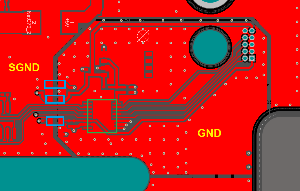
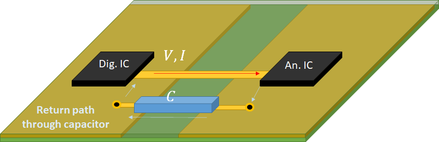
Noise reduction analog techniques begin with partitioning the board into analog and digital zones. Route analog signals exclusively over analog ground areas to keep return currents local and quiet. Digital zones handle switching noise separately, preventing spillover. A continuous ground plane, split only if necessary, maintains low impedance while allowing isolation. When splitting, connect planes at a single point under mixed-signal devices to avoid loops. Ground loops form when multiple paths exist between grounds, picking up magnetic fields or allowing current sharing that induces noise.
To eliminate ground loops analog, adopt a star grounding topology where all returns converge at one point, often near the power entry or primary converter. This single-point connection ensures no circular current paths. In practice, use wide traces or vias to the star point, minimizing resistance. For multilayer boards, stitching vias along partition boundaries tie layers together, providing low-inductance paths. Guard traces around sensitive analog lines, referenced to analog ground, further shield from adjacent noise. These techniques collectively suppress common-mode and differential noise.
Decoupling capacitors play a key role in analog grounding by shunting high-frequency noise to ground. Place low-ESR ceramics close to IC power pins, with one side directly on the ground plane. Multiple values, from 0.01 μF to 10 μF, bypass different frequency bands. In noisy environments, ferrite beads on supply lines isolate sections. For precision analog, reference oscillators and clocks to the analog ground to minimize jitter. Regular design reviews verify these implementations prevent noise coupling.
Best Practices for Mixed-Signal Grounding
Mixed-signal grounding demands careful integration of analog and digital domains. Prefer a single partitioned ground plane over fully split planes to avoid high-inductance crossings. Partition boundaries should follow natural circuit divisions, with no traces spanning the gap. Under mixed-signal ICs like ADCs, bridge the partition with a narrow trace or vias for low-impedance connection. Connect separate AGND and DGND pins externally at the package to the analog plane, isolating digital currents. This approach confines noise while maintaining reference integrity.
In multilayer stackups, dedicate inner layers to analog and digital grounds, adjacent to their respective signals. IPC-6012E specifications ensure plane performance through qualification tests for continuity and impedance. Vias stitching planes every few millimeters reduce slot radiation. For power distribution, separate analog and digital supplies, filtering before analog sections. Route high-current digital returns away from analog areas. Engineers benefit from simulating PDN impedance to validate low peaks across frequencies.
Layout discipline reinforces these practices. Place mixed-signal devices near partition centers for short bridges. Use 30-40% ground pins on connectors to lower impedance. Avoid right angles in ground pours; use smooth curves or fills. Post-layout checks for unbroken planes under traces ensure compliance. These steps align with structured engineering workflows for reliable mixed-signal boards.
Troubleshooting Common Grounding Issues in Analog PCBs
Engineers often encounter noise despite solid ground planes due to overlooked details. Excessive digital switching noise invading analog sections signals poor partitioning. Verify no analog traces enter digital zones and returns stay local. Ground bounce from inadequate decoupling appears as periodic spurs; add capacitors and check placement. Measure plane impedance with TDR to identify high spots from voids or thin copper.
Ground loops manifest as 50/60 Hz hum from external fields. Trace multiple chassis or shield connections and consolidate to star points. In prototypes, sockets add inductance; switch to direct soldering for production. Simulate current flow to predict hot spots causing gradients. IPC-A-600K criteria help inspect plane acceptability for uniformity. Systematic debugging, starting from power entry, resolves most issues.
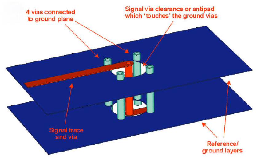
Return path disruptions from slits under traces increase EMI. Fill gaps with stitching or reroute. For high-speed analog, verify stripline integrity with ground planes on both sides. Field probing identifies coupling paths. Document fixes for iterative improvements.
Conclusion
Effective PCB ground plane analog circuits design hinges on principled implementation of ground planes, partitioning, and loop avoidance. Analog grounding techniques like star points, stitching, and dedicated planes deliver noise reduction analog benefits essential for precision. Mixed-signal grounding succeeds through disciplined layout and single-point connections. Adhering to standards ensures manufacturability and performance. Electric engineers applying these strategies achieve cleaner signals, lower emissions, and robust systems. Prioritize grounding early in the design cycle for optimal results.
FAQs
Q1: What are the primary analog grounding techniques for PCB ground plane analog circuits?
A1: Analog grounding techniques emphasize partitioned ground planes with analog sections under sensitive signals and single-point connections to digital areas. Use stitching vias along boundaries and decoupling capacitors near ICs to shunt noise. Route returns locally to minimize impedance. This setup, aligned with design standards, prevents digital transients from corrupting analog performance, ensuring low noise floors.
Q2: How do you achieve noise reduction analog using ground planes?
A2: Noise reduction analog relies on continuous copper pours providing low-impedance returns and shielding. Partition boards to isolate analog from digital noise sources, bridging only at star points. Adjacent power-ground layers offer decoupling capacitance. Guard traces and proper via placement further suppress coupling. Verify with impedance checks for uniform potential.
Q3: What causes ground loops analog and how to prevent them in mixed-signal grounding?
A3: Ground loops analog arise from multiple ground paths allowing induced currents or shared impedance. Prevent them with star grounding, converging all returns at one point near power or converters. Avoid splits under traces; use bridges if needed. In mixed-signal grounding, connect AGND/DGND externally to the analog plane. This maintains reference integrity without loops.
Q4: Why is partitioning critical for mixed-signal grounding on PCBs?
A4: Partitioning in mixed-signal grounding confines digital return currents to digital zones, preventing noise injection into analog paths. Route signals strictly within zones and connect planes at low-impedance points under devices. Multilayer stackups with dedicated planes enhance isolation. This technique reduces crosstalk and EMI, vital for data converters and sensors.
References
IPC-2221A — Generic Standard on Printed Board Design. IPC
IPC-6012E — Qualification and Performance Specification for Rigid Printed Boards. IPC, 2015
IPC-A-600K — Acceptability of Printed Boards. IPC, 2020


