Introduction
PCB trace routing forms the backbone of any printed circuit board design, directly influencing signal integrity, electromagnetic compatibility, and overall performance. Engineers must carefully plan trace paths to handle high-speed signals, power distribution, and control impedance while adhering to manufacturing constraints. Poor routing can lead to crosstalk, reflections, and failures in high-frequency applications, making it a critical skill for electric engineers. This article explores routing topologies, techniques like manual routing and autorouting, and best practices for differential pairs, serpentine routing, minimizing vias, layer stackup, ground planes, and crosstalk mitigation. By mastering these elements, designers can create reliable boards that meet demanding electrical requirements. Understanding these principles ensures optimized PCB trace routing from concept to production.
What Is PCB Trace Routing and Why It Matters
PCB trace routing involves laying out conductive paths, or traces, on the board to connect components electrically. These traces carry signals, power, and ground, with their geometry affecting electrical characteristics like resistance, capacitance, and inductance. Routing decisions impact signal speed, noise levels, and thermal performance, especially in dense, multi-layer boards. In high-speed designs, improper PCB trace routing can cause timing skew, increased insertion loss, or electromagnetic interference that violates compliance standards.
The relevance of effective routing topologies and techniques cannot be overstated in modern electronics. As clock rates exceed gigahertz and board densities rise, signal integrity becomes paramount. Autorouting tools offer speed, but manual routing provides precision for critical nets. Factors like layer stackup and ground planes further define routing success, ensuring low crosstalk and stable reference planes for return currents. Ultimately, skilled PCB trace routing minimizes risks, reduces iterations, and enhances product reliability for electric engineers.
Key Routing Topologies
Routing topologies define how traces connect multiple points, each suited to specific applications like power delivery or data buses. Point-to-point topology links two components directly, ideal for simple, low-speed signals where minimal delay matters. Daisy chain routing connects devices in series, common for address lines or clock distribution to multiple loads, but it introduces cumulative delays that require careful length management.
Star or point-to-star topology fans traces from a central driver to each receiver, preserving signal timing across loads at the cost of fanout congestion. Tree topology branches from a spine, balancing load distribution for balanced transmission lines. For power and ground, mesh or grid topologies provide low-impedance paths, while solid planes offer the lowest inductance. Selecting the right topology in PCB trace routing depends on signal type, speed, and board constraints.
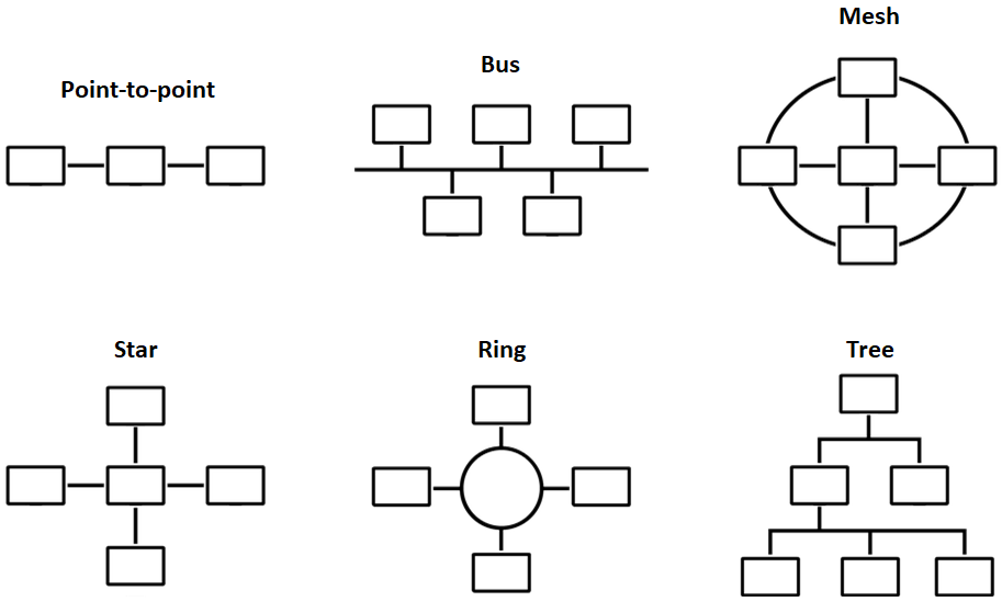
In differential signaling, paired traces follow symmetric topologies to maintain balance. Length-matched pairs in daisy chain or fly-by configurations support protocols like PCIe or DDR memory. Engineers must evaluate topology trade-offs, such as area usage versus performance, during initial layout planning.
Essential Routing Techniques
Manual routing allows engineers full control, enabling optimization for impedance, length matching, and via minimization on complex boards. Designers route critical nets first, such as clocks and high-speed data, before filling with lower-priority traces. This technique excels in multi-layer designs where layer stackup influences coupling and crosstalk.
Autorouting automates trace placement using predefined rules, speeding up initial layouts for high-density boards. However, it often requires post-editing to fix violations like excessive vias or acute angles that cause reflections. Hybrid approaches combine both, with manual intervention for differential pairs and buses. Effective PCB trace routing blends these techniques based on design complexity and deadlines.
Differential pairs demand tight coupling, routed as parallel traces with controlled spacing and length matching to preserve signal balance. Gaps larger than three times the trace width increase common-mode noise susceptibility. Serpentine routing equalizes lengths for timing-critical nets, using smooth S-shaped bends to avoid sharp turns that introduce stubs.
Best Practices for PCB Trace Routing
Adhering to best practices ensures robust PCB trace routing across topologies and techniques. Start with trace width calculations for current capacity and impedance, following IPC-2221 guidelines for external and internal layers. Maintain clearances at least three times the trace width between adjacent signals to reduce fringing fields and crosstalk.
Minimize vias by planning layer transitions strategically; each via adds inductance and capacitance that degrade high-speed performance. Use blind or buried vias in multi-layer boards to shorten paths without penetrating all layers. Layer stackup planning pairs signal layers adjacent to ground planes, providing low-inductance return paths and shielding.
Ground planes act as reference for microstrip and stripline traces, minimizing loop inductance and radiation. Split planes carefully to avoid crossing high-speed signals, and use stitching vias every lambda/20 to tie planes together. For crosstalk mitigation, orthogonal routing on adjacent layers reduces parallel run lengths, while guard traces ground potential coupling paths.
Route high-speed traces as striplines between planes for better confinement than microstrips. Avoid 90-degree bends; use 45-degree or curved corners to prevent reflections. In dense areas, teardrops at pads ease manufacturing stress per IPC-6012 performance specs.
Advanced Considerations in Routing
For high-frequency designs, simulate impedance pre-layout using field solvers to match transmission line targets. Differential pairs benefit from accordion tuning for fine length adjustments without excessive serpentine meanders. Power routing employs wide traces or planes, with decoupling capacitors placed via stitching to local references.
Troubleshooting routing issues involves checking eye diagrams for jitter and attenuation. Common pitfalls include unmatched lengths in buses causing skew, or vias too close to bends amplifying resonances. Iterative DRC runs catch violations early.
Layer transitions for signals require symmetric via structures, like back-drilled stubs, to control impedance discontinuities. Ground bounce in multi-drop buses favors series termination at the source.
Conclusion
Mastering PCB trace routing topologies, techniques, and best practices elevates design quality and performance. From daisy chain and star configurations to manual routing, autorouting, differential pairs, and serpentine methods, each element contributes to signal integrity. Prioritizing minimizing vias, optimal layer stackup, solid ground planes, and crosstalk control ensures reliable operation. Electric engineers who integrate these principles reduce EMI risks and fabrication yields improve. Apply these guidelines systematically for superior boards in demanding applications.
FAQs
Q1: What are the main advantages of manual routing over autorouting in PCB trace routing?
A1: Manual routing offers precise control for high-speed nets, allowing engineers to optimize differential pairs, minimize vias, and adhere to layer stackup rules. It excels in complex topologies where autorouting may create inefficient paths or increase crosstalk. While time-intensive, it reduces post-layout fixes and improves signal integrity overall.
Q2: How does serpentine routing help in high-speed PCB designs?
A2: Serpentine routing equalizes trace lengths for timing-critical signals like clocks or data buses, preventing skew in differential pairs. Engineers create controlled meanders with smooth bends to avoid reflections, maintaining impedance consistency. This technique is essential for DDR or PCIe interfaces requiring matched propagation delays.
Q3: Why is minimizing vias important in PCB trace routing?
A3: Vias introduce parasitic inductance and capacitance, degrading high-speed signal quality and increasing crosstalk risks. Fewer vias shorten paths, preserve return currents via adjacent ground planes, and simplify fabrication. Strategic placement aligns with layer stackup for optimal performance.
Q4: How do ground planes reduce crosstalk in routing topologies?
A4: Ground planes provide shielding and low-impedance return paths, confining fields between signal layers to minimize coupling. In daisy chain or star topologies, stitching vias maintain plane continuity, reducing loop areas. Proper integration per design standards enhances EMI control.
References
IPC-2221B - Generic Standard on Printed Board Design. IPC, 2009
IPC-6012E - Qualification and Performance Specification for Rigid Printed Boards. IPC, 2017
IPC-A-600K - Acceptability of Printed Boards. IPC, 2020


