Introduction
High-speed PCB designs face significant challenges in maintaining signal integrity as data rates increase beyond several gigabits per second. Impedance control emerges as a fundamental technique to ensure predictable signal propagation, while crosstalk represents a primary source of noise that degrades performance. The interplay between impedance control and crosstalk becomes critical, as mismatches in characteristic impedance lead to reflections that exacerbate coupling between adjacent traces. This comprehensive analysis explores impedance control crosstalk dynamics, highlighting how controlled impedance PCBs mitigate these issues. Engineers must grasp these relationships to optimize designs for reliability and speed. By examining technical principles and practical strategies, this article provides actionable insights for electric engineers tackling signal integrity problems.
Understanding Impedance Control in PCBs
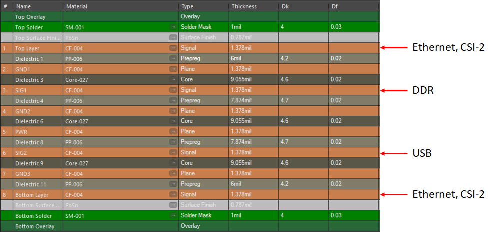
Impedance control refers to the process of designing PCB traces to maintain a specific characteristic impedance, typically 50 ohms for single-ended lines or 100 ohms for differential pairs. Characteristic impedance arises from the interaction of inductance and capacitance per unit length in transmission lines, governed by the formula Z0 equals square root of L over C. In controlled impedance PCBs, factors such as trace width, thickness, dielectric height, and material properties are precisely managed during fabrication. This control prevents signal distortion in high-frequency applications where wavelengths approach trace dimensions. Without proper impedance matching to drivers and receivers, voltage standing waves form, leading to overshoot and ringing. IPC-2141A outlines guidelines for achieving consistent impedance in high-speed designs.
Related Reading: The Impact of Impedance Control on Crosstalk: A Comprehensive Analysis
The Nature of Crosstalk in High-Speed PCBs
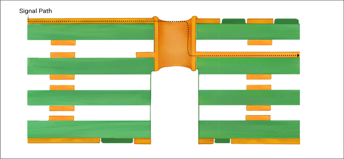
Crosstalk occurs when electromagnetic fields from an aggressor trace induce unwanted voltages or currents on a nearby victim trace. It manifests in two primary forms: near-end crosstalk (NEXT), which appears at the aggressor end, and far-end crosstalk (FEXT), observed at the victim receiver. Capacitive coupling dominates for electric fields between traces, while inductive coupling arises from shared magnetic flux. The magnitude depends on trace geometry, spacing, length of parallel runs, and rise times of signals. In dense layouts, these effects accumulate, potentially causing bit errors or timing violations. Effective crosstalk management requires minimizing coupling coefficients alongside impedance control.
Mechanisms Linking Impedance Control to Crosstalk
Impedance discontinuities, such as varying trace widths or plane splits, cause partial reflections of the incident signal according to the reflection coefficient formula, gamma equals (Z_load minus Z0) over (Z_load plus Z0). These reflected waves propagate backward and can recouple to adjacent traces, amplifying crosstalk beyond direct coupling. In impedance control crosstalk scenarios, poor Z0 uniformity turns minor inductive or capacitive interactions into significant noise sources. For instance, a reflected edge from the aggressor aligns temporally with the victim signal, constructively interfering and peaking noise levels. Signal reflections crosstalk thus compound, as multiple bounces create a noisy waveform envelope. Maintaining tight impedance tolerances, often within 10 percent, disrupts this feedback loop.
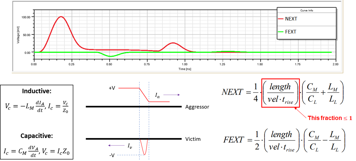
Reflections and Their Role in Crosstalk Amplification
Signal reflections crosstalk intensifies when impedance mismatches create echoes that overlap with coupled noise. In a typical scenario, an aggressor trace launches a fast edge, part of which couples capacitively to the victim while the remainder reflects due to a via or bend. The reflected portion travels back, partially recouples forward along the victim, and arrives delayed at the receiver. This delay matches the propagation time over parallel sections, leading to peak-to-peak noise swings proportional to coupling strength times reflection coefficient. Controlled impedance PCBs reduce this by minimizing gamma, ensuring clean propagation with damped transients. Engineers observe this in time-domain reflectometry traces, where low VSWR indicates effective control.
Quantitative Insights into Impedance-Crosstalk Interactions
Crosstalk voltage approximates as V_xtalk equals (coupling capacitance over total capacitance) times dV/dt times length, modulated by impedance mismatches. Reflections add a factor of (1 plus gamma) to effective aggressor amplitude for the victim. In simulations, varying Z0 by 20 percent can double peak crosstalk compared to matched cases. Differential pairs benefit doubly, as balanced impedance suppresses common-mode coupling. Practical limits emerge from stackup variations during lamination, underscoring the need for test coupons. IPC-6012E specifies qualification tests ensuring impedance performance aligns with design intent.
Best Practices for Implementing Impedance Control
Design stackups with symmetric layers around signal traces to stabilize dielectric constants and minimize warpage effects on impedance. Select materials with low loss tangents for high frequencies, and calculate trace geometries using field solvers validated against IPC-2141A equations. Maintain minimum spacing per 3W rule, where W is trace width, to decouple traces while preserving impedance. Incorporate reference planes fully under high-speed nets, avoiding splits larger than trace width. Verify post-fabrication with TDR or VNA measurements on coupons placed near critical nets. These steps ensure controlled impedance PCBs deliver low crosstalk in production volumes.
Verification and Testing Strategies
Fabrication tolerances demand robust verification to confirm impedance control crosstalk targets. Embed TDR launch points on panels for inline testing, targeting deviations under 10 percent. Simulate pre-layout with 3D solvers accounting for solder mask and surface roughness effects. Post-etch inspection confirms width uniformity, as etch factor influences Z0. For assembled boards, eye diagram analysis quantifies combined reflections and crosstalk impacts. Adhering to IPC-TM-650 methods standardizes these processes across suppliers.
Case Study: High-Speed SerDes Interface Optimization
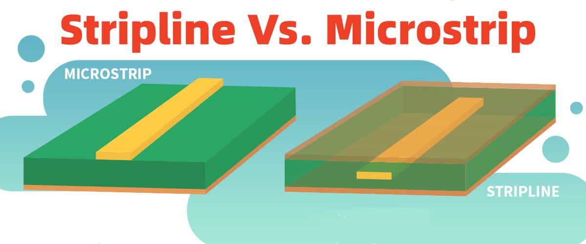
Consider a 25 Gbps SerDes channel pair on a multilayer PCB, where initial uncontrolled impedance led to 15 percent NEXT exceeding eye mask margins. Analysis revealed 15 percent Z0 variation from asymmetric stackup, causing reflections that boosted coupled noise. Redesigning for stripline routing with 100-ohm differential control, uniform 5 mil dielectric, and guarded ground planes reduced peak crosstalk by over 50 percent in simulation. Fabrication coupons confirmed 8 percent tolerance, passing signal integrity validation. This adjustment enabled compliance without retiming or equalization overhead. Such outcomes underscore impedance control's direct impact on crosstalk budgets.
Advanced Techniques for Dense Designs
Guard traces or stitching vias shield sensitive nets, further isolating coupling paths. Differential routing preserves odd-mode impedance while rejecting even-mode noise. Frequency-domain analysis reveals crosstalk peaks at harmonics, guiding length matching. Material advancements like low-Dk cores aid impedance stability in HDI boards. Integrating these with impedance control forms a holistic signal integrity strategy.
Related Reading: Shielding Strategies: Effective Crosstalk Reduction for Sensitive Circuits
Conclusion
Impedance control stands as a cornerstone in combating crosstalk within high-speed PCBs, directly curbing reflections that amplify noise coupling. Controlled impedance PCBs ensure signal fidelity by matching transmission line characteristics to system needs, minimizing signal reflections crosstalk effects. Engineers benefit from structured design per industry guidelines, verification rigor, and layout discipline. Implementing these principles yields robust performance, fewer iterations, and reliable operation at elevated data rates. Prioritizing impedance control crosstalk mitigation unlocks the full potential of modern electronics.
FAQs
Q1: What is the relationship between impedance control and crosstalk in PCBs?
A1: Impedance control maintains consistent characteristic impedance to prevent reflections, which otherwise recouple to adjacent traces and intensify crosstalk. In controlled impedance PCBs, uniform Z0 reduces gamma, limiting noise amplification from NEXT and FEXT. Poor control leads to ringing that overlaps with coupled signals, degrading eye diagrams. Engineers achieve lower bit error rates by targeting tolerances under 10 percent during design and fabrication.
Q2: How does impedance mismatch contribute to signal reflections crosstalk?
A2: Impedance mismatch generates reflections per the reflection coefficient, sending backward waves that recouple forward along victim lines. These delayed components constructively add to direct crosstalk, peaking noise at receivers. Signal reflections crosstalk thus scales with discontinuity severity and parallel run lengths. Mitigation involves matching Z0 across vias, bends, and transitions for clean propagation.
Q3: What are best practices for designing controlled impedance PCBs to reduce crosstalk?
A3: Optimize stackups for symmetric dielectrics, calculate trace widths via IPC-2141A equations, and enforce 3W spacing rules. Use full reference planes and verify with TDR coupons. Guard traces further decouple nets. These ensure impedance control crosstalk stays within budgets for high-speed integrity.
Q4: Which standards guide impedance control in PCB design?
A4: IPC-2141A provides design guidelines for high-speed controlled impedance circuit boards, including calculation methods. IPC-6012E specifies performance qualifications for rigid boards with impedance requirements. IPC-2251 addresses packaging for high-speed logic, covering crosstalk and impedance management. These ensure standardized, reliable implementations.
References
IPC-2141A — Design Guide for High-Speed Controlled Impedance Circuit Boards. IPC.
IPC-6012E — Qualification and Performance Specification for Rigid Printed Boards. IPC, 2017.
IPC-2251 — Design Guide for the Packaging of High Speed Logic. IPC.