Introduction
In the realm of printed circuit board (PCB) design, vias play a critical role in ensuring electrical connectivity between layers. For electrical engineers working on high-speed applications, via design directly influences signal integrity and overall performance during PCB prototyping. Poorly designed vias can introduce signal loss, impedance mismatches, and crosstalk, which are detrimental to system reliability. This article explores the nuances of PCB via types, including blind and buried vias, and their impact on performance. Key considerations such as the via stub effect, backdrilling vias, and high-speed via design principles are discussed to guide engineers in optimizing prototypes. By understanding these factors, designers can minimize signal degradation and achieve robust performance in modern electronics.
What Are PCB Vias and Why Do They Matter?
Vias are small conductive pathways that connect different layers of a multilayer PCB. They allow signals and power to travel vertically through the board, enabling complex routing in compact designs. For electrical engineers, the importance of vias extends beyond mere connectivity. In high-speed designs, vias can act as points of signal discontinuity if not properly engineered. Signal loss, reflections, and electromagnetic interference often originate from suboptimal via structures. As data rates increase in applications like telecommunications and computing, the need for precise via design becomes paramount. Standards such as IPC-6012E provide guidelines for via implementation to ensure reliability. Without attention to these details during PCB prototyping, engineers risk performance issues that could delay product development.
Technical Principles of Via Design and Signal Loss
Understanding Signal Loss in Vias
Signal loss in vias occurs due to several factors, including impedance mismatches and parasitic effects. When a high-speed signal transitions through a via, any discontinuity in the signal path can cause reflections. These reflections degrade signal quality, especially at frequencies above a few gigahertz. The length and diameter of the via, along with the surrounding dielectric material, influence these effects. Engineers must consider the via's aspect ratio, which is the ratio of its depth to diameter, to minimize loss as outlined in IPC-A-600K.
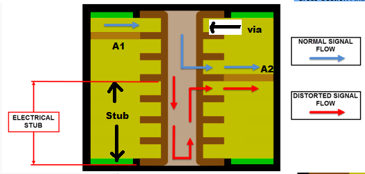
The Via Stub Effect
One significant contributor to signal degradation is the via stub effect. A via stub is the unused portion of a via that extends beyond the signal path. This stub acts as an open-ended transmission line, causing resonance and signal reflections at specific frequencies. The longer the stub, the lower the resonant frequency, which can interfere with high-speed signals. Mitigating the via stub effect is crucial for maintaining signal integrity in PCB prototyping.
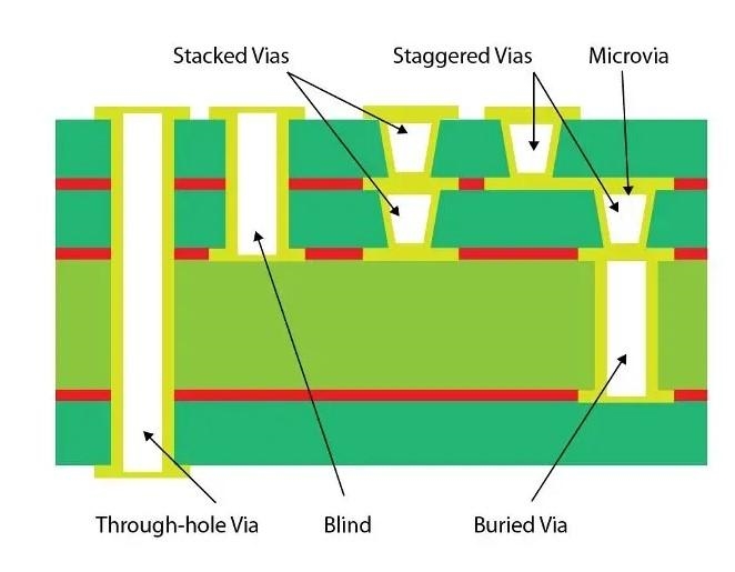
Types of PCB Vias and Their Impact
Different PCB via types offer unique advantages and challenges in high-speed designs. Through-hole vias, which span the entire board thickness, are simple but often result in long stubs. Blind vias connect an outer layer to an inner layer without penetrating the full board, reducing stub length. Buried vias connect internal layers only, further optimizing space and signal performance. Each type affects signal loss differently due to variations in geometry and electrical characteristics. Choosing the right via type during prototyping can significantly enhance performance.
Related Reading: Outer Layer Copper Thickness and Via Design: Best Practices for Reliable PCB Interconnects
Practical Solutions for High-Speed Via Design
Minimizing the Via Stub Effect
To address the via stub effect, engineers can adopt several strategies. Shortening the stub length by careful layer planning is a primary approach. Using blind and buried vias instead of through-hole vias reduces unused via portions. Additionally, optimizing the via placement to align with signal layers minimizes stub formation. These practices, supported by guidelines in IPC-6012E, help maintain signal integrity during high-speed via design.
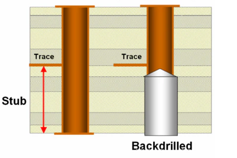
Implementing Backdrilling Vias
Backdrilling vias is a manufacturing technique used to remove the unused stub portion of a through-hole via. By drilling out the excess via material after initial fabrication, engineers can eliminate the resonant stub effect. This method is particularly effective in high-speed designs where signal frequencies exceed several gigahertz. Backdrilling requires precise control to avoid damaging the functional via section, and adherence to standards like IPC-A-600K ensures quality. This approach is a valuable tool in PCB prototyping for performance-critical applications.
Optimizing Blind and Buried Vias
Blind and buried vias are essential for high-density and high-speed designs. Blind vias save space by connecting only necessary layers, while buried vias enable internal routing without surface exposure. Both types reduce signal loss by limiting stub lengths and minimizing parasitic capacitance. However, their fabrication requires advanced processes, and engineers must ensure compliance with manufacturing tolerances specified in IPC-6012E. Proper use of these vias during prototyping can lead to compact, high-performance boards.
Related Reading: High Reliability Blind Via Design: Meeting Stringent Industry Standards
Design Guidelines for High-Speed Vias
For high-speed via design, several best practices should be followed. First, maintain consistent impedance by matching via dimensions to trace characteristics. Second, place ground vias near signal vias to provide a return path and reduce crosstalk. Third, use simulation tools to model via behavior under high-frequency conditions. These steps, aligned with industry standards like JEDEC J-STD-020E for component integration, help engineers anticipate and mitigate signal loss. Careful attention to via placement and stackup design is vital in prototyping phases.
Troubleshooting Via-Related Issues in Prototyping
During PCB prototyping, via-related issues can manifest as signal distortion or unexpected failures. Engineers often encounter challenges like excessive crosstalk or impedance discontinuities. To troubleshoot, start by reviewing the via stub length and type used in the design. If stubs are present, consider backdrilling or switching to blind and buried vias. Signal integrity analysis using simulation tools can identify problem areas before fabrication. Additionally, ensure that via aspect ratios comply with limits set in IPC-A-600K to prevent manufacturing defects. Iterative testing and refinement during prototyping are key to resolving these issues and achieving optimal performance.
Conclusion
Via design is a critical factor in rapid PCB prototyping, especially for high-speed applications where signal loss can compromise performance. Understanding the via stub effect, leveraging techniques like backdrilling vias, and selecting appropriate PCB via types such as blind and buried vias are essential steps. By following best practices in high-speed via design and adhering to recognized standards, electrical engineers can minimize signal degradation and enhance reliability. Thoughtful via implementation during the prototyping phase ensures that the final PCB design meets the stringent demands of modern electronics, paving the way for successful product development.
FAQs
Q1: What is the via stub effect, and how does it impact high-speed PCB designs?
A1: The via stub effect occurs when an unused portion of a via acts as a resonant structure, causing signal reflections. In high-speed PCB designs, this can degrade signal integrity, especially at higher frequencies. Engineers can mitigate this by using shorter stubs, blind vias, or backdrilling techniques to remove excess via material, ensuring better performance as per industry guidelines.
Q2: How do blind and buried vias improve PCB prototyping outcomes?
A2: Blind and buried vias reduce signal loss by minimizing stub lengths and optimizing layer connectivity. Blind vias connect outer to inner layers, while buried vias link internal layers, saving space. This enhances high-density designs during PCB prototyping, allowing for compact layouts and improved signal quality when designed according to established manufacturing standards.
Q3: Why is backdrilling vias important for high-speed via design?
A3: Backdrilling vias removes unused stub portions in through-hole vias, eliminating resonance that causes signal loss. This technique is crucial in high-speed via design to maintain signal integrity at gigahertz frequencies. It requires precise manufacturing control but significantly boosts performance, making it a valuable step in prototyping critical boards.
Q4: How can engineers optimize high-speed via design during prototyping?
A4: Engineers can optimize high-speed via design by matching via impedance to traces, using ground vias for return paths, and selecting appropriate PCB via types. Simulation tools help predict signal behavior, while adherence to standards ensures manufacturability. Careful layer planning and stub minimization are also key to reducing signal loss in prototypes.
References
IPC-6012E — Qualification and Performance Specification for Rigid Printed Boards. IPC, 2020.
IPC-A-600K — Acceptability of Printed Boards. IPC, 2020.
JEDEC J-STD-020E — Moisture/Reflow Sensitivity Classification. JEDEC, 2014.


