Introduction
In the realm of printed circuit board (PCB) design, selecting the appropriate PCB design software stands as a foundational decision for electric engineers. Modern electronics demand intricate layouts that handle high-speed signals, dense component placement, and thermal constraints, making PCB layout tools indispensable for achieving reliable outcomes. The right PCB software not only streamlines the design process but also minimizes errors that could lead to costly prototypes or field failures. Engineers must weigh factors like simulation capabilities, rule enforcement, and integration with manufacturing data to ensure efficiency. This article explores the critical aspects of PCB software comparison, highlighting why thoughtful selection drives project success. By focusing on proven engineering principles, designers can align their choice with industry demands for precision and performance.
Understanding PCB Layout Software and Its Role
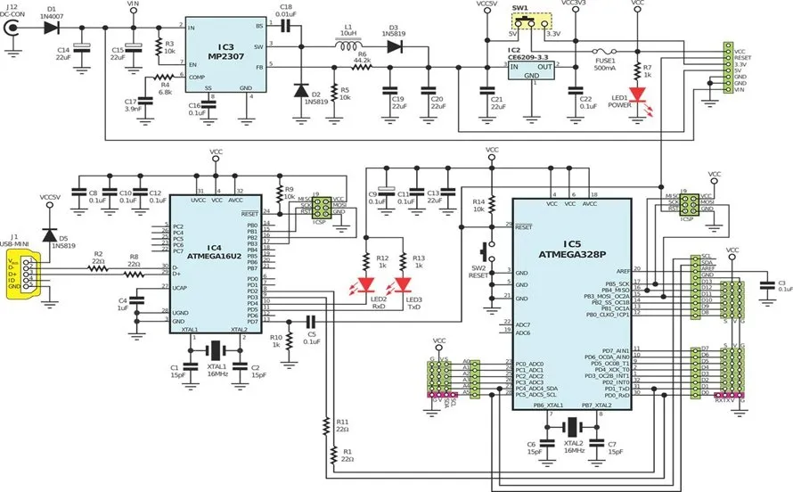
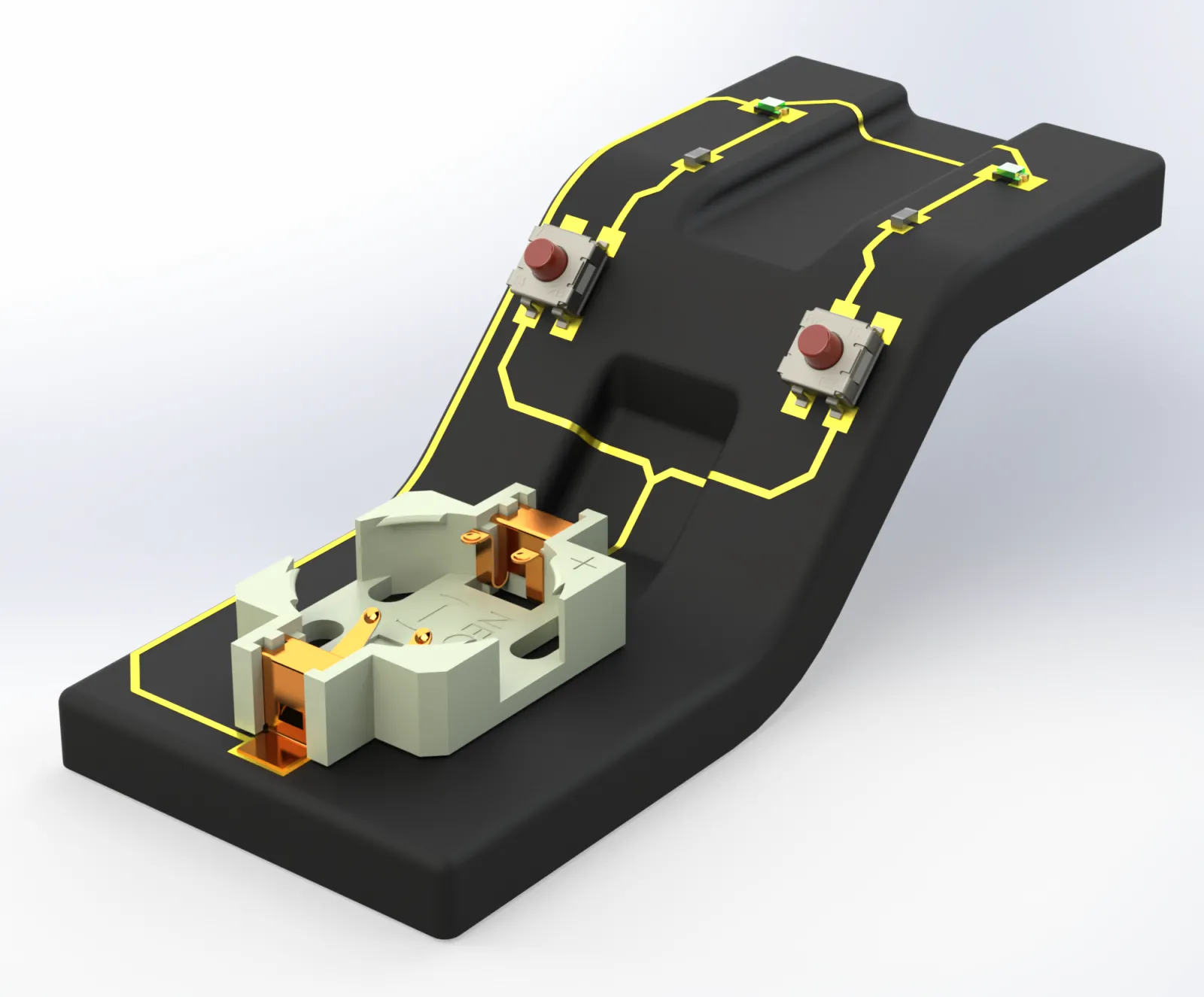
PCB layout software encompasses a suite of digital tools used to transform schematic diagrams into physical board layouts ready for fabrication. These PCB design software platforms handle tasks such as component placement, trace routing, and layer stackup definition, all while enforcing design rules for manufacturability. At its core, the software automates repetitive processes, allowing engineers to focus on innovation rather than manual drafting. Without robust PCB layout tools, designs risk issues like signal crosstalk or inadequate power distribution, which compromise functionality.
The relevance of choosing the best PCB software extends to every phase of the product lifecycle. Poorly selected tools can inflate design cycles by up to weeks, as engineers grapple with inadequate features for complex boards. In contrast, well-equipped PCB design software integrates checks for impedance control and thermal vias, aligning with standards like IPC-2221 for generic printed board design. This ensures boards meet performance specs from the outset. Moreover, as board densities increase with miniaturization trends, scalable PCB layout tools become essential for handling multilayer configurations without performance lags. Ultimately, the right software bridges the gap between concept and production, safeguarding quality and reducing iteration costs.
Key Technical Features in PCB Design Software
Effective PCB layout tools incorporate advanced algorithms for autorouting that respect electrical constraints, such as differential pair matching and length tuning for high-speed interfaces. Engineers benefit from real-time design rule checks (DRC) that flag violations in clearance, via sizing, and pad spacing, preventing downstream fabrication rejects. Multilayer support is crucial, enabling precise stackup visualization to manage crosstalk and return paths effectively. Simulation integration within the PCB software allows preliminary analysis of signal integrity (SI) and power integrity (PI), predicting behaviors before prototyping.
Thermal management features further elevate the best PCB software, with tools for copper pour optimization and via thermal relief generation. These capabilities ensure heat dissipation aligns with component ratings, avoiding hotspots in power-heavy designs. Library management systems streamline component data handling, supporting standardized land patterns to facilitate assembly. For high-reliability applications, advanced PCB design software includes constraint-driven routing that enforces minimum bend radii and annular ring widths per industry guidelines. Such features collectively enhance design accuracy, making PCB software comparison hinge on depth of these technical implementations.
Layer stackup planning represents another pivotal mechanism in PCB layout tools. Software must model material properties, dielectric thicknesses, and prepreg sequences to calculate controlled impedances accurately. This process directly influences signal propagation speeds and attenuation, critical for gigabit Ethernet or DDR memory interfaces. Engineers rely on built-in calculators to iterate stackups swiftly, ensuring compliance with performance specifications. Without precise modeling, boards may exhibit unexpected resonances or losses, underscoring the need for sophisticated simulation kernels in PCB design software.
Criteria for PCB Software Comparison and Selection
When conducting a PCB software comparison, engineers prioritize scalability to handle board sizes from prototypes to production volumes. Entry-level tools may suffice for simple single-layer boards, but complex designs demand robust solvers for fanout and escape routing on fine-pitch BGAs. Performance metrics, such as routing completion times and memory usage, become decisive for large-scale projects. User interface intuitiveness reduces training overhead, enabling teams to collaborate seamlessly via version control integrations.
Cost-effectiveness forms a key pillar in evaluating the best PCB software, balancing upfront licensing with long-term productivity gains. Open architecture for third-party plugins extends functionality, such as adding custom DRC rules or export formats for fabrication. Data management features, including intelligent part search and bill-of-materials (BOM) generation, streamline handoff to procurement and assembly. In PCB layout tools, output fidelity to Gerber and ODB++ formats ensures seamless translation to CAM processes, minimizing interpretation errors at the fabricator.
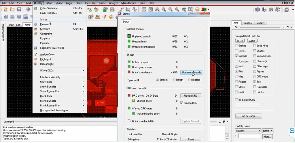
Best practices for selection involve trial evaluations under real workloads, assessing crash resilience and undo depth. Engineers should verify support for emerging standards like J-STD-001 for soldering requirements, which influences assembly-ready outputs. Integration with mechanical CAD for enclosure fit checks prevents redesign loops. A structured PCB software comparison matrix, evaluating these facets quantitatively, guides decisions toward tools that amplify engineering throughput without sacrificing precision.
- Routing Engine
- Essential Criteria: Constraint-driven, multi-net optimization
- Impact on Design Workflow: Reduces iteration cycles for dense boards
- Simulation Tools
- Essential Criteria: SI/PI analysis, thermal modeling
- Impact on Design Workflow: Predicts failures pre-prototype
- Library Handling
- Essential Criteria: Parametric footprints, 3D models
- Impact on Design Workflow: Accelerates component placement
- Output Formats
- Essential Criteria: IPC-D-356 netlists, extended Gerbers
- Impact on Design Workflow: Ensures fab compatibility
- Performance
- Essential Criteria: Large board handling (>100 layers)
- Impact on Design Workflow: Supports enterprise-scale projects
Challenges and Practical Insights in PCB Layout
Electric engineers often encounter hurdles like inadequate high-speed modeling in basic PCB design software, leading to suboptimal via transitions or stub lengths. Troubleshooting involves upgrading to tools with field-solver accuracy for S-parameter extraction, vital for RF and microwave boards. Case in point: a hypothetical multilayer server board design required precise 50-ohm impedance control across 16 layers; initial software lacked fanout automation, extending layout time by days until a more capable PCB layout tool was adopted.
Another insight revolves around collaborative workflows, where cloud-enabled PCB software facilitates distributed teams in reviewing revisions. Version tracking prevents overwrite conflicts, preserving design history. For DFM, proactive checks against IPC-A-600 acceptability criteria catch issues like excessive solder mask dams early. These practices underscore how the right PCB layout tools mitigate risks in fast-paced development cycles.
Conclusion
Choosing the right PCB design software profoundly influences design quality, efficiency, and manufacturability for electric engineers. By prioritizing features like advanced routing, simulation, and standards compliance, teams unlock streamlined workflows and reduced errors. PCB software comparison reveals that scalability and integration outweigh superficial appeal, ensuring alignment with complex project needs. Investing time in evaluation pays dividends through fewer prototypes and faster time-to-market. Ultimately, the best PCB software empowers engineers to deliver robust, high-performance boards that meet industry rigors.
FAQs
Q1: What features define the best PCB software for high-speed designs?
A1: The best PCB software excels in constraint-driven routing, integrated SI/PI simulation, and precise impedance calculators for differential pairs. It supports length matching and via optimization to minimize reflections, adhering to engineering principles for gigabit signals. Robust DRC enforces spacing rules, while 3D stackup viewers aid crosstalk analysis. These elements ensure reliable performance in demanding applications, streamlining PCB software comparison for electric engineers.
Q2: How do PCB layout tools impact manufacturing yield?
A2: PCB layout tools directly boost yield by embedding DFM checks for annular rings, clearances, and panelization. They generate accurate Gerbers and drill files, reducing fab rejects from misinterpretations. Features like teardrop pads and thermal reliefs enhance solder joint integrity per soldering standards. Engineers using advanced tools report fewer iterations, making thoughtful selection in PCB design software a yield multiplier.
Q3: What should engineers consider in a PCB software comparison?
A3: In PCB software comparison, assess routing speed, library depth, simulation accuracy, and output compatibility. Evaluate scalability for multilayer boards and user training ease to fit team dynamics. Cost versus feature ROI, plus update frequency for new component support, guides choices. Prioritize tools with strong constraint managers for custom rules, ensuring versatility across projects.
Q4: Why is library management critical in PCB design software?
A4: Library management in PCB design software centralizes footprints, symbols, and 3D models, slashing placement errors. Parametric editors allow quick adaptations for variants, supporting standardized land patterns. Integrated search and validation prevent mismatches during layout. This foundation accelerates design cycles and maintains consistency, a key differentiator in PCB layout tools.
References
IPC-2221B — Generic Standard on Printed Board Design. IPC, 2012
IPC-A-600K — Acceptability of Printed Boards. IPC, 2020
J-STD-001H — Requirements for Soldered Electrical and Electronic Assemblies. IPC/JEDEC, 2018


