Introduction
Multilayer printed circuit boards (PCBs) are the backbone of modern electronics, enabling compact designs with high functionality in devices ranging from smartphones to industrial systems. As the complexity of these boards increases with multiple layers, ensuring their reliability and performance becomes a critical challenge for engineers. Test and measurement in multilayer PCB development play a pivotal role in verifying design integrity, detecting defects, and maintaining quality. Techniques such as signal integrity testing and PCB design verification help identify issues early, reducing costly failures. This article explores why PCB test and measurement is essential, delving into technical principles, practical approaches, and industry standards that guide multilayer PCB testing. Aimed at electric engineers, the content provides structured insights into achieving robust designs through effective testing methodologies.
Why Test and Measurement Matters in Multilayer PCB Development
Multilayer PCBs, with their stacked conductive layers separated by insulating materials, support dense component layouts and intricate signal paths. However, this complexity introduces risks such as signal degradation, crosstalk, and manufacturing defects. Test and measurement are vital to ensure that these boards meet performance expectations under real-world conditions. Without rigorous PCB testing techniques, issues like impedance mismatches or interlayer shorts can compromise functionality, leading to system failures. For electric engineers, multilayer PCB test processes validate design assumptions, confirm manufacturing precision, and ensure compliance with stringent industry standards. By prioritizing PCB test and measurement, teams can avoid expensive redesigns, maintain product reliability, and meet project timelines, ultimately safeguarding end-user satisfaction in high-stakes applications like aerospace or medical equipment.
Technical Principles of Test and Measurement in Multilayer PCBs
Understanding Signal Integrity in Multilayer Designs
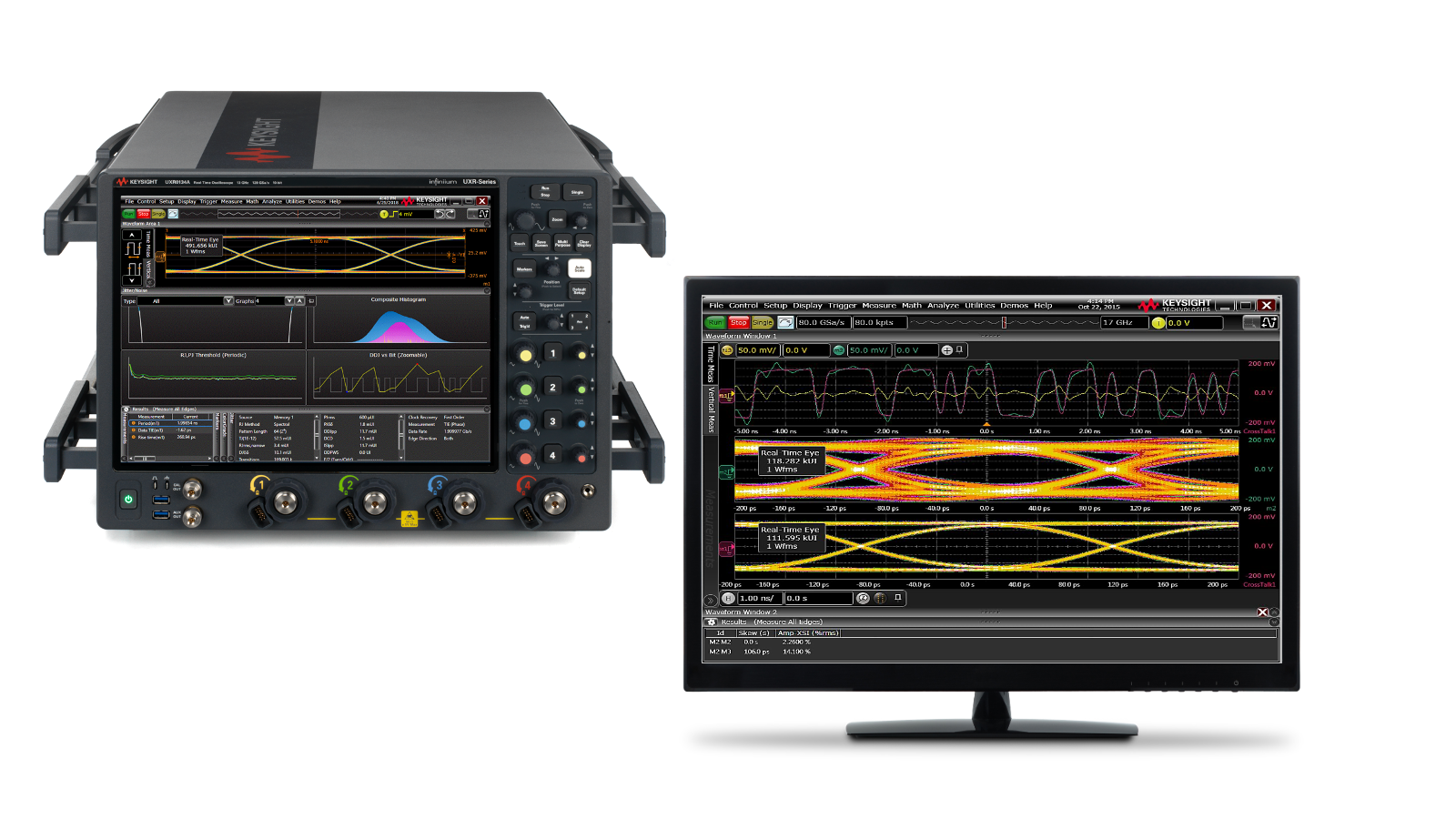
Signal integrity is a cornerstone of multilayer PCB performance, especially in high-speed applications. It refers to the ability of a signal to travel through the board without distortion, noise, or loss. In multilayer designs, factors like trace length, layer transitions, and dielectric properties impact signal quality. Signal integrity test methods measure parameters such as impedance, reflection, and crosstalk using tools like time-domain reflectometry (TDR) and vector network analyzers (VNA). These tests help engineers identify mismatches or discontinuities that could degrade performance. Standards such as IPC-2141A provide guidelines for controlled impedance design, ensuring consistency in test approaches. Proper signal integrity testing prevents data errors in high-frequency circuits, a common concern in telecommunications and computing systems.
Related Reading: Signal Integrity PCB Designers
Electrical Testing for Layer Interconnections
Multilayer PCBs rely on vias and interlayer connections to route signals across different planes. Defects in these connections, such as open circuits or shorts, can render a board unusable. Electrical testing, often guided by IPC-TM-650 test methods, evaluates continuity and insulation resistance between layers. Techniques like flying probe testing and in-circuit testing (ICT) are widely used to detect faults without damaging the board. These multilayer PCB test approaches ensure that all conductive paths function as intended, a critical step before assembly. Engineers must also consider thermal stress effects on interconnections, as outlined in IPC-6012E, to predict long-term reliability under operating conditions.
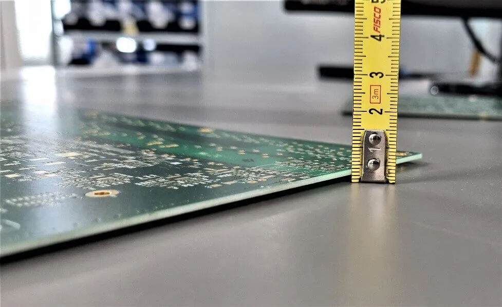
Mechanical and Environmental Testing
Beyond electrical performance, multilayer PCBs must withstand mechanical stress and environmental factors. Warpage, delamination, and thermal expansion are common issues that can disrupt functionality. Mechanical testing, based on standards like IPC-TM-650, measures board flatness and structural integrity using tools such as dial gauges or laser scanners. Environmental tests assess performance under humidity, temperature cycling, and vibration, following guidelines from JEDEC J-STD-020E for moisture sensitivity. These tests are crucial for applications in harsh environments, ensuring that the PCB maintains its form and function over time. For engineers, integrating mechanical and environmental checks into the PCB design verification process is essential for robust outcomes.
Practical PCB Testing Techniques for Multilayer Designs
Design Verification Through Simulation and Prototyping
PCB design verification starts early in the development cycle, often through simulation tools that model signal behavior and thermal distribution. These simulations predict potential issues like signal delays or hotspots before physical prototypes are built. Once a prototype is available, engineers apply PCB testing techniques such as boundary scan testing to validate digital circuits. Following standards like IPC-2221B, which covers design requirements for multilayer boards, ensures that verification aligns with industry best practices. Early detection of design flaws through these methods saves time and resources, allowing for adjustments before mass production.
In-Process Testing During Manufacturing
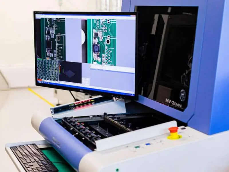
During manufacturing, in-process testing monitors the quality of each layer and interconnection. Techniques such as automated optical inspection (AOI) check for surface defects, while microsectioning, as per IPC-A-600K, evaluates internal layer alignment and via integrity. These multilayer PCB test methods catch deviations in real time, preventing defective boards from reaching assembly. Engineers must adhere to acceptance criteria outlined in IPC-6012E to maintain consistency across production batches. Regular calibration of test equipment, aligned with ISO 9001:2015 quality management principles, further enhances accuracy in manufacturing environments.
Post-Production Functional Testing
After manufacturing, functional testing verifies that the multilayer PCB performs as intended under simulated operating conditions. This includes power-up tests, signal integrity checks, and stress testing to mimic real-world usage. Signal integrity test protocols, often supported by IPC-2141A guidelines, ensure that high-speed signals remain stable. Functional testing also validates compliance with end-application requirements, a critical step for industries like automotive or medical where reliability is non-negotiable. For electric engineers, documenting test results per IPC standards provides traceability and accountability in case of field failures.
Best Practices for Effective Test and Measurement
To maximize the benefits of PCB test and measurement, engineers should adopt a systematic approach. First, define clear test objectives based on the board’s application and performance requirements. Use industry standards like IPC-TM-650 to select appropriate test methods for electrical, mechanical, and environmental parameters. Second, invest in calibrated equipment to ensure measurement accuracy, adhering to ISO 9001:2015 for quality assurance. Third, integrate testing at every stage, from design verification to post-production, to catch issues early. Finally, maintain detailed records of test data for future reference and compliance audits. These practices, rooted in recognized standards, help build reliable multilayer PCBs that meet stringent demands.
Insight: Addressing Challenges in High-Density Multilayer Designs
High-density multilayer PCBs, often used in advanced electronics, pose unique test and measurement challenges. With tighter trace spacing and smaller vias, signal integrity issues become more pronounced, requiring precise testing tools. Engineers must also account for thermal management, as densely packed components generate significant heat. Following IPC-2221B design guidelines, teams can optimize layer stackups to minimize interference. Additionally, leveraging advanced multilayer PCB test techniques like high-frequency probing ensures accurate assessment of signal behavior. For electric engineers, staying updated on evolving standards and test methodologies is key to tackling the complexities of modern PCB designs.
Conclusion
Test and measurement are indispensable in multilayer PCB development, ensuring that these complex boards meet performance, reliability, and quality expectations. From signal integrity tests to mechanical evaluations, each testing phase addresses specific risks associated with multilayer designs. By adhering to established industry standards and employing practical PCB testing techniques, engineers can mitigate failures and deliver robust solutions. As electronics continue to evolve, the role of PCB design verification and multilayer PCB test processes will only grow, demanding continuous learning and adaptation. For electric engineers, mastering these practices is essential to drive innovation while maintaining the highest standards of excellence.
FAQs
Q1: What is the role of signal integrity test in multilayer PCB development?
A1: Signal integrity test ensures that signals in multilayer PCBs travel without distortion or noise, critical for high-speed applications. It measures impedance, crosstalk, and reflections using specialized tools. Following standards like IPC-2141A, engineers can validate performance and prevent data errors. This testing is vital during PCB design verification to confirm that the board supports intended frequencies and maintains reliability in demanding environments.
Q2: How do PCB testing techniques improve multilayer PCB quality?
A2: PCB testing techniques, such as flying probe testing and automated optical inspection, detect defects like shorts or misalignments in multilayer PCBs. Guided by IPC-TM-650, these methods ensure electrical and structural integrity at various stages. By identifying issues early, they reduce rework costs and enhance reliability. Consistent testing leads to boards that meet application needs and comply with industry benchmarks.
Q3: Why is PCB design verification critical for multilayer boards?
A3: PCB design verification confirms that multilayer board layouts meet performance and manufacturability requirements before production. Using simulations and prototype testing, engineers identify signal or thermal issues early. Standards like IPC-2221B provide a framework for validation. This process minimizes design flaws, ensuring the final product functions reliably in complex applications while saving time and resources during development.
Q4: What standards guide multilayer PCB test processes?
A4: Multilayer PCB test processes are guided by standards such as IPC-6012E for performance specifications, IPC-TM-650 for test methods, and IPC-A-600K for acceptability criteria. ISO 9001:2015 ensures quality management in testing practices. JEDEC J-STD-020E addresses environmental stress testing. These standards provide consistent, reliable frameworks for engineers to validate board quality and performance across development stages.
References
IPC-2141A — Design Guide for High-Speed Controlled Impedance Circuit Boards. IPC, 2004.
IPC-2221B — Generic Standard on Printed Board Design. IPC, 2012.
IPC-6012E — Qualification and Performance Specification for Rigid Printed Boards. IPC, 2020.
IPC-A-600K — Acceptability of Printed Boards. IPC, 2020.
IPC-TM-650 — Test Methods Manual for Printed Circuit Boards. IPC, Current Revision.
JEDEC J-STD-020E — Moisture/Reflow Sensitivity Classification for Nonhermetic Surface Mount Devices. JEDEC, 2014.
ISO 9001:2015 — Quality Management Systems. ISO, 2015.


