Introduction
Surface Mount Technology (SMT) assembly forms the backbone of modern electronics production, enabling compact, high-density printed circuit boards (PCBs). Design for Manufacturing (DFM) integrates manufacturability considerations early in the PCB design phase to ensure smooth transitions from prototype to high-volume production. Poor DFM practices often lead to assembly defects, yield losses, and increased costs during SMT processes like solder paste printing, component placement, and reflow soldering. Engineers focusing on DFM guidelines for SMT can minimize issues such as bridging, tombstoning, and insufficient solder joints. This article explores practical strategies for PCB layout for SMT, component placement optimization, and solder joint design DFM, drawing on established industry principles to guide electric engineers toward reliable outcomes. By prioritizing these elements, teams achieve higher first-pass yields and faster time-to-market.
DFM refers to the systematic approach of designing PCBs to align with the capabilities and constraints of SMT assembly equipment and processes. In SMT, this involves optimizing layouts for automated pick-and-place machines, stencil printers, and reflow ovens while anticipating potential failure modes. Effective DFM reduces rework, scrap rates, and production delays by addressing manufacturability from the outset. It bridges the gap between design intent and factory realities, ensuring components are placed accurately and soldered reliably. For electric engineers, understanding DFM means evaluating trade-offs in density versus processability early. Ultimately, strong DFM practices enhance overall product quality and support scalable manufacturing.
What is Design for Manufacturing (DFM) in SMT Assembly?
The relevance of DFM intensifies with shrinking component sizes and higher assembly densities in today's devices. Without proper DFM, even well-designed circuits face challenges like misalignment or thermal imbalances during reflow. Industry standards reinforce these principles, providing benchmarks for consistent results across facilities. Engineers who incorporate DFM iteratively during layout revisions avoid costly respins. This proactive mindset shifts focus from fixing problems post-assembly to preventing them entirely.
Key DFM Guidelines for SMT Assembly
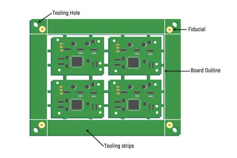
DFM guidelines for SMT emphasize simplicity, standardization, and predictability in design choices. Start with board outlines that avoid sharp corners or excessive protrusions, which complicate handling and fixturing in assembly lines. Include fiducial marks in corners and near critical areas to enable precise machine alignment during placement. Panelization rules promote efficient use of production panels by specifying breakaway tabs, v-scoring, or tab routing compatible with depaneling tools. Copper balance across layers prevents warpage during reflow, a common issue in multilayer boards. Adhering to these guidelines streamlines the entire SMT workflow from printing to inspection.
Silkscreen and solder mask applications also fall under DFM scrutiny. Ensure reference designators are legible and positioned away from pads to avoid stencil interference or inspection obscuration. Solder mask expansion over pads must account for registration tolerances to prevent exposure or bridging risks. These details, often overlooked, directly impact paste release and joint formation. Regular design reviews against DFM checklists catch deviations early. Practical implementation involves collaborating with assembly partners during the design phase for feedback on specific capabilities.
PCB Layout for SMT: Foundational Considerations
PCB layout for SMT requires balancing signal integrity, thermal management, and assembly flow. Route traces to minimize vias under components, as excess vias can trap solder or cause head-in-pillow defects during reflow. Group components by process type, placing fine-pitch parts in dedicated zones to match machine capabilities. Orient polarized components consistently to speed up placement programming and reduce errors. Layout symmetry aids in even heating, crucial for preventing lift-offs in reflow profiles. Engineers should simulate airflow over the board to identify hot spots that could warp substrates.
Edge clearance from the board perimeter supports conveyor handling and prevents components from interfering with rails. Test points and connectors positioned thoughtfully allow access without obstructing pick-and-place heads. Layer stackups influence overall flatness, with balanced core and prepreg thicknesses mitigating bow and twist. These layout strategies form the bedrock of successful SMT runs. Troubleshooting starts here, as layout flaws propagate through every assembly step.
Component Placement Optimization in SMT
Component placement optimization drives efficiency and reliability in SMT assembly. Maintain adequate spacing between parts to allow clean solder paste deposition and prevent bridging during reflow. Align similar components in the same direction to simplify feeder setup and reduce rotation errors on pick-and-place machines. Prioritize taller components along board edges or in less dense areas to avoid shadowing during printing or inspection. Thermal-sensitive parts benefit from placement away from high-power dissipators, ensuring uniform heating. Height mapping across the board helps predict reflow behavior and adjust oven profiles accordingly.
Fine-pitch devices demand zoned placement, separating them from larger parts to match nozzle sizes and vision systems. Avoid placing components under overhangs or in corners where access proves challenging. Optimization also considers downstream processes like conformal coating or potting, positioning parts to facilitate even coverage. Engineers troubleshoot placement issues by reviewing machine data logs for offsets or collisions. Consistent application of these rules boosts throughput and yield.
Solder Joint Design DFM: Critical for Reliability
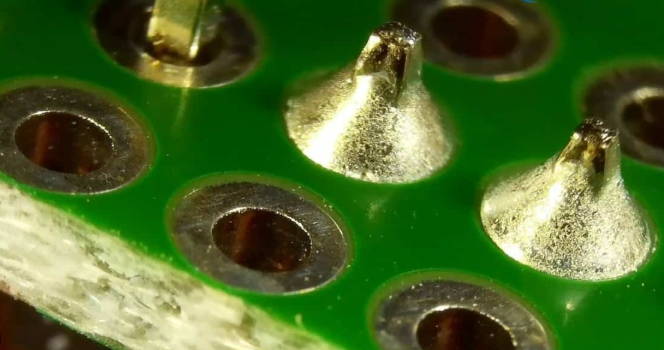
Solder joint design DFM focuses on land patterns, paste volume, and profile compatibility to form robust connections. Land geometries per IPC-7351B ensure optimal solder wetting and fillet formation without excess or deficiency. Stencil apertures should release paste uniformly, avoiding apertures smaller than component leads to prevent insufficient volume. Bridging risks increase with tight pitches, so mask-defined pads help contain solder flow. Joint quality aligns with IPC-A-610J acceptability criteria, targeting smooth heel-toe fillets and full barrel fills.
Reflow dynamics influence joint integrity, with rapid ramps risking voids or opens. Balanced thermal mass around joints promotes even melting, reducing tombstoning in chip resistors. Troubleshooting poor joints often traces back to pad finish choices like ENIG or HASL, which affect spreadability. DFM here means validating designs through paste-in-place simulations before production. Reliable joints withstand vibration, thermal cycling, and handling stresses over the product lifecycle.
Stencil and Solder Paste DFM Practices
Stencil design complements PCB layout for precise paste application. Thinner foils paired with appropriate thickness ratios improve release for fine features. Trapezoidal apertures reduce paste smear, enhancing volume control on small pads. Avoid overly complex cutouts that trap residue, complicating cleaning cycles. Paste selection considers particle size distribution for high-density boards, ensuring flow without slumping.
Registration tolerances between stencil and board demand robust fiducials and flatness. Pressure settings during printing must accommodate varying pad sizes. Troubleshooting print defects involves inspecting volume uniformity with SPI tools early. These practices directly feed into placement accuracy and reflow success.
Reflow Soldering and Thermal DFM Factors
Reflow soldering DFM accounts for board warpage, component coplanarity, and profile tolerances. IPC J-STD-001J outlines requirements for soldered assemblies, emphasizing process controls. Preheat zones remove flux volatiles gradually, preventing spattering. Peak temperatures must melt solder without damaging components, with soak times balancing activity levels. Cooling rates control grain structure for joint strength. Warped boards lift edges, misaligning joints, so DFM stresses symmetric layouts.
Thermal profiling verifies zone effectiveness across board sizes. Troubleshooting hotspots involves adjusting conveyor speed or nitrogen use. These factors ensure defect-free runs at scale.
DFM Checklist for SMT Assembly
A comprehensive DFM checklist SMT streamlines reviews. Verify board outline and panelization compatibility first. Check component spacing, orientation, and height mapping next. Confirm land patterns and stencil rules align. Review fiducials, silkscreen, and mask clearances. Assess thermal balance and edge support. Simulate paste volume and reflow risks. Finalize with test point access and documentation completeness. Use this sequentially to catch issues proactively.
- Board dimensions and shape feasibility
- Fiducial placement and quantity
- Component spacing per pitch class
- Consistent orientation for polarized parts
- Land pattern adherence to standards
- Solder mask and silkscreen offsets
- Thermal symmetry across layers
- Edge clearance for handling
Regular checklist use prevents oversights, especially in complex designs.
Troubleshooting Common SMT DFM Issues
Tombstoning arises from uneven heating, resolved by optimizing land proportions and profiles. Bridging stems from excess paste, fixed via stencil tuning or spacing increases. Insufficient wetting points to surface contamination or poor pad design, addressed through cleanliness protocols. Head-in-pillow defects link to coplanarity mismatches, mitigated by placement force adjustments. Warpage troubleshooting involves stackup reviews and baking before assembly. Data-driven analysis from AOI and X-ray pinpoints root causes quickly. Iterative DFM refinements based on trial runs yield long-term gains.
Conclusion
DFM plays a pivotal role in achieving successful SMT assembly by embedding manufacturability into every design decision. From PCB layout for SMT to component placement optimization and solder joint design DFM, these practices minimize defects and maximize yields. A structured DFM checklist SMT serves as an invaluable tool for electric engineers navigating production challenges. Adhering to standards like IPC-A-610J and IPC J-STD-001J ensures consistency and reliability. Prioritizing DFM not only cuts costs but also accelerates market delivery, fostering robust electronics. Teams that master these elements position themselves for efficient, scalable manufacturing.
FAQs
Q1: What are the primary DFM guidelines for SMT to prevent assembly defects?
A1: DFM guidelines for SMT stress adequate component spacing, proper fiducial placement, and balanced thermal layouts to avoid bridging and tombstoning. Land patterns must support uniform solder volume, while board edges ensure handling clearance. Stencil design optimizes paste release, and consistent orientations speed placement. Following these reduces rework and boosts first-pass yields in production.
Q2: How does component placement optimization improve SMT outcomes?
A2: Component placement optimization groups parts by size and process, maintains spacing for machine access, and aligns orientations for efficiency. It prevents shadowing in printing and ensures even reflow heating. Troubleshooting focuses on height variations and edge proximity. This approach enhances accuracy, throughput, and joint reliability across runs.
Q3: Why is solder joint design DFM essential in PCB layout for SMT?
A3: Solder joint design DFM defines land geometries for proper wetting and fillet formation, critical for mechanical and electrical integrity. It considers paste volume and reflow dynamics to meet acceptability criteria. Poor design leads to voids or cracks under stress. Optimizing this in PCB layout for SMT ensures durable connections without excessive rework.
Q4: What should a DFM checklist SMT include for quick reviews?
A4: A DFM checklist SMT covers board outline feasibility, fiducials, spacing rules, land patterns, mask offsets, and thermal balance. It verifies stencil compatibility and test access too. Use it pre-tapeout to flag issues early. This practical tool supports troubleshooting and consistent high-yield assembly.
References
IPC J-STD-001J — Requirements for Soldered Electrical and Electronic Assemblies. IPC, 2024
IPC-A-610J — Acceptability of Electronic Assemblies. IPC, 2024
IPC-7351B — Generic Requirements for Surface Mount Design and Land Pattern Standard. IPC, 2010


