Introduction
In high-density PCB designs, via-in-pad configurations enable tighter routing and support fine-pitch components like BGAs. These vias, placed directly within surface mount pads, demand special attention during PCB assembly to ensure robust solder joints. Via filling materials play a critical role in enhancing via-in-pad reliability by providing mechanical support, preventing solder intrusion, and minimizing surface irregularities. Without proper filling, issues such as outgassing or uneven reflow can compromise assembly yields. This article explores how conductive epoxy and non-conductive epoxy address these challenges, offering practical insights for electric engineers troubleshooting reliability in demanding applications. Understanding these mechanisms helps optimize designs for consistent performance.
What Is Via-in-Pad and Why Via Filling Matters
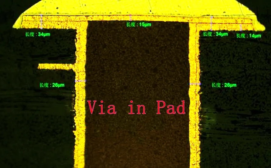
Via-in-pad refers to a plating structure where a via hole intersects a component pad, allowing direct connection without additional breakout space. This technique is essential for HDI boards and BGA fanout, maximizing board real estate. However, during PCB assembly, unfilled vias can trap flux residues or allow molten solder to wick into the barrel, leading to voids or weak joints. Via filling materials seal the via completely, creating a planar surface that promotes uniform solder wetting. Reliability improves as filled vias resist thermal cycling stresses and mechanical shock better than open ones. For electric engineers, selecting the right via filling approach directly impacts assembly success rates and long-term field performance.
The relevance stems from evolving assembly processes like lead-free reflow, which expose boards to higher temperatures and steeper ramp rates. Unfilled vias may exhibit planarity issues up to several mils, disrupting stencil printing and solder paste deposition. Filled vias mitigate these by eliminating depressions, ensuring consistent volume of solder paste. In production environments, this translates to fewer defects during inspection and higher first-pass yields. Moreover, via-in-pad reliability becomes paramount in applications with vibration or thermal excursions, where joint integrity prevents intermittent failures.
Technical Principles Behind Via Filling and Reliability
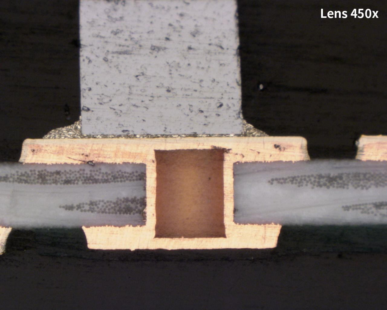
Via filling works by displacing air and plating residues within the via barrel, using materials matched to the PCB's thermal expansion profile. Conductive epoxy, formulated with silver or copper particles, provides electrical continuity and heat dissipation paths, ideal for power or high-speed signals. Non-conductive epoxy, typically resin-based, offers structural reinforcement without shorting adjacent traces. Both cure to form a solid plug that withstands reflow peaks around 260°C, but material choice hinges on CTE compatibility with copper and laminate. Mismatched CTE leads to cracking under thermal stress, compromising via-in-pad reliability.
During PCB assembly, reliability hinges on outgassing behavior as temperatures rise. Epoxy fills with low moisture absorption prevent vapor expansion that could delaminate the pad or create blowholes in solder joints. Standards like IPC-4761 classify via protection types, specifying fill coverage for Type IV and VI configurations common in via-in-pad. These guidelines ensure the plug extends beyond the via walls, providing robust capping. Engineers must consider plating thickness too, as thin copper barrels risk cracking if the fill exerts excessive pressure during cure.
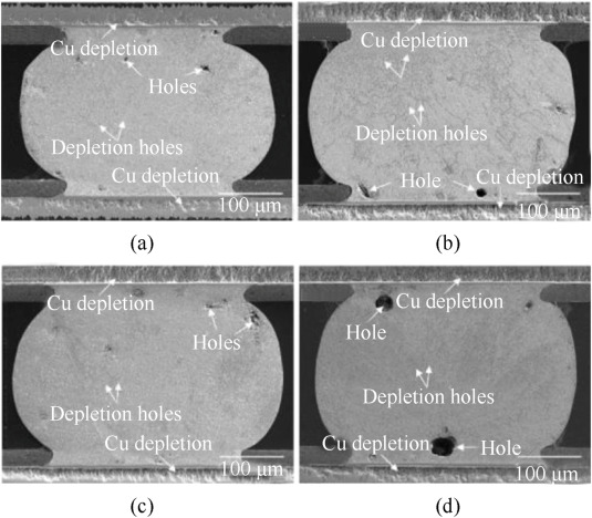
Mechanical integrity further depends on fill density and adhesion. Incomplete fills leave voids that act as stress concentrators, accelerating fatigue in thermal cycling tests. Conductive fills enhance current carrying by paralleling the barrel plating, reducing resistance rise over cycles. Non-conductive options prioritize insulation, preventing dendritic growth in humid environments. Cross-section analysis reveals optimal fills exhibit uniform distribution without air pockets, correlating to higher via-in-pad reliability metrics.
Thermal management principles also influence fill selection. Vias in pad often serve as heat sinks for BGAs, where conductive epoxy conducts heat away from hotspots. Simulations show filled vias lower junction temperatures by distributing flux evenly. However, overfilled pads can cause doming, altering stencil release and paste volume. Balancing fill height to match pad coplanarity is key, typically verified via laser profilometry before assembly.
Practical Solutions and Best Practices for Via Filling
Start with design rules that accommodate via-in-pad processing: pad diameter at least 0.15 mm larger than finished hole size per IPC-6012 guidelines for Class 3 boards. Specify fill type in fabrication notes, distinguishing conductive epoxy for thermal vias versus non-conductive for signal integrity. During procurement, request cross-section coupons to verify 100% fill and flatness within 0.075 mm tolerance. These practices ensure via-in-pad reliability translates from fab to assembly line.
In PCB assembly, preheat boards to drive off moisture from fills, reducing outgassing risks per J-STD-001 requirements for soldering. Use nitrogen reflow atmospheres to inhibit oxidation on exposed copper caps over fills. Post-reflow X-ray inspection flags voids or bridging caused by incomplete plugs. Troubleshooting incomplete fills involves adjusting epoxy viscosity and cure profiles, often lowering ramp rates to 1-2°C/s. Engineers report yield improvements exceeding 95% with these tweaks.
Material selection follows application needs. For BGA escape vias, non-conductive epoxy suffices for mechanical planarity, avoiding conductivity-induced crosstalk. Conductive epoxy suits ground or power planes, maintaining low impedance. Test compatibility via thermal shock cycles, monitoring for cracks via dye-and-peel. Hybrid approaches, like partial copper electroplating before epoxy, boost reliability in stacked vias.
Process controls include via cleaning post-drill to remove smear, ensuring epoxy bonds directly to plating. Cure under vacuum minimizes voids, with post-cure bake at 150°C for 2 hours stabilizing the fill. Capping with solder mask or plating prevents contamination during handling. These steps align with IPC-A-600 acceptability criteria for Class 2/3 products.
Troubleshooting Common Via-in-Pad Reliability Issues
Engineers often encounter solder beading from marginal fills, where epoxy shrinkage leaves shallow dimples attracting excess paste. Shear testing reveals joint strength drops 20-30% in such cases; remedy by overfilling slightly and lapping flat. Delamination signals CTE mismatch, diagnosed via acoustic microscopy showing lift-off at interfaces. Switch to low-CTE epoxies or reinforce with plated caps.
Outgassing manifests as popcorning during reflow, popping flux boils from trapped volatiles. Bake boards at 125°C for 24 hours pre-assembly to equilibrate. For conductive fills, monitor electromigration under bias, as particle settling can create hot spots. Non-conductive fills fare better here but watch for CAF precursors in high-voltage designs.
Warpage exacerbates via stress in large panels; filled vias reduce asymmetric expansion. Use shadow moiré for quantification, targeting <50 μm bow/twist. If failures persist, revert to dogbone escapes for prototyping, graduating to filled via-in-pad once process is dialed in.
Conclusion
Via filling profoundly elevates via-in-pad reliability by addressing planarity, outgassing, and stress vulnerabilities in PCB assembly. Conductive epoxy excels in thermal/electrical paths, while non-conductive epoxy prioritizes structural integrity. Adhering to standards like IPC-4761 and IPC-6012 ensures consistent outcomes. Practical troubleshooting refines processes, boosting yields and durability. Electric engineers benefit from integrating these strategies early, yielding robust assemblies for critical applications.
FAQs
Q1: What are the main via filling materials used for via-in-pad reliability?
A1: Conductive epoxy with metal particles enhances electrical and thermal performance, while non-conductive epoxy provides mechanical support without conductivity. Selection depends on signal type and heat dissipation needs. Both seal vias to prevent solder wicking during PCB assembly. Proper curing ensures planarity for fine-pitch soldering.
Q2: How does non-conductive epoxy improve via-in-pad reliability in PCB assembly?
A2: It creates a flat pad surface, avoiding solder voids from depressions. Low outgassing during reflow minimizes defects like blowholes. CTE matching reduces cracking under thermal cycles. Inspect cross-sections to confirm full fill. This boosts joint strength per J-STD-001 criteria.
Q3: When should conductive epoxy be chosen over non-conductive for via filling?
A3: Opt for conductive epoxy in power or ground vias needing low resistance paths. It parallels barrel plating for better current handling. Avoid in high-speed signals to prevent crosstalk. Thermal simulations guide decisions for via-in-pad reliability.
Q4: What common failures occur without proper via filling in via-in-pad designs?
A4: Solder wicking creates weak joints, outgassing causes popcorning, and voids accelerate fatigue. Uneven surfaces disrupt stencil printing. Thermal mismatch leads to cracks. Pre-assembly baking and profilometry mitigate these in PCB assembly flows.
References
IPC-4761 - Via Protection and Covering for Printed Boards. IPC, 2013
IPC-6012E - Qualification and Performance Specification for Rigid Printed Boards. IPC, 2015
J-STD-001H - Requirements for Soldered Electrical and Electronic Assemblies. IPC, 2018
IPC-A-600K - Acceptability of Printed Boards. IPC, 2020


