Introduction
Rigid PCB design forms the backbone of most electronic products, from consumer devices to industrial controls. Engineers often invest significant time in schematic capture and layout, yet small oversights can lead to manufacturing failures, assembly issues, or field returns. A comprehensive rigid PCB design checklist serves as a critical safeguard, helping teams systematically identify and eliminate rigid PCB design errors before production. This approach ensures compliance with industry expectations and minimizes costly respins. By incorporating rigid PCB design review steps early, designers can validate signal integrity, thermal performance, and manufacturability. Ultimately, mastering rigid PCB design validation and verification transforms potential pitfalls into reliable boards ready for high-volume assembly.
In today's fast-paced development cycles, skipping thorough checks amplifies risks like trace shorts, via failures, or impedance mismatches. These rigid PCB design mistakes not only inflate costs but also delay time-to-market. This article provides a structured rigid PCB design checklist tailored for electric engineers, drawing on proven engineering principles. Follow it to streamline your workflow and achieve flawless results. Whether reviewing a multilayer board or optimizing for high-speed signals, these guidelines promote precision and efficiency.
Why a Rigid PCB Design Checklist Matters
Rigid printed circuit boards demand meticulous planning due to their fixed structure and complex interactions between layers. Without a rigid PCB design checklist, common oversights cascade into fabrication rejects or assembly headaches. For instance, inadequate clearances can cause shorts during plating, while poor routing leads to signal crosstalk. Engineers benefit from this systematic review by catching issues pre-prototype, saving up to significant rework expenses. Industry data underscores that design flaws account for a large portion of PCB failures, emphasizing proactive verification.
Adopting a checklist aligns with engineering best practices, fostering consistency across teams. It covers schematic integrity, physical layout, and design rule compliance, reducing variability in outcomes. For electric engineers handling high-reliability applications, this tool ensures boards meet performance under thermal stress or vibration. Regular use builds institutional knowledge, accelerating future projects. In essence, a rigid PCB design review checklist elevates design quality from good to exceptional.
Key Principles of Rigid PCB Design
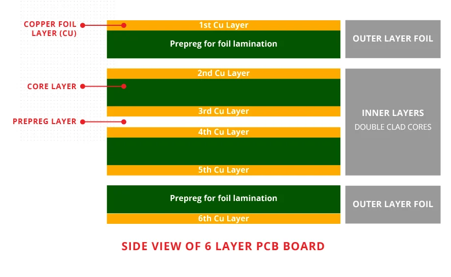
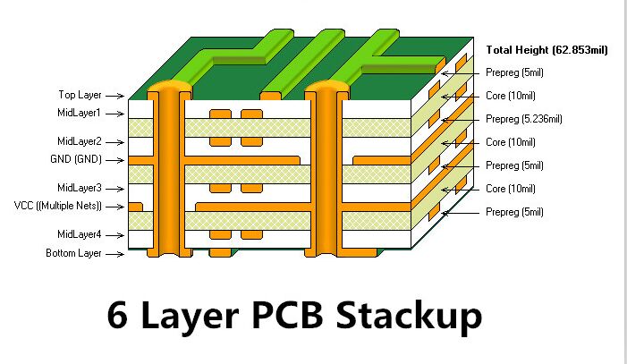
Rigid PCB design revolves around balancing electrical, mechanical, and thermal requirements within a rigid laminate structure. Core elements include material selection, layer stackup, and interconnect strategies like vias and traces. Copper distribution must support current flow without excessive heating, while dielectric properties control capacitance and impedance. Engineers must consider board thickness uniformity to prevent warpage during reflow soldering. Adhering to established guidelines ensures the board functions reliably across its lifecycle.
Layer count influences complexity, with multilayer boards requiring precise registration for blind and buried vias. Signal routing demands length matching for differential pairs to maintain timing integrity. Power planes provide low-impedance distribution but introduce challenges in splitting for noise isolation. Thermal vias under high-power components dissipate heat effectively into inner layers. These principles form the foundation for any rigid PCB design validation process.
Fabrication tolerances play a pivotal role, as drill breakout or annular ring deficiencies compromise reliability. Solder mask alignment protects traces while enabling precise component mounting. Silkscreen legends aid assembly without interfering with test points. By internalizing these mechanisms, designers preempt rigid PCB design errors rooted in oversight.
The Ultimate Rigid PCB Design Checklist
This rigid PCB design checklist breaks down into phases: pre-layout, layout, post-layout, and final review. Each step includes verification actions to catch potential issues early. Use it as a living document, adapting to project specifics while prioritizing manufacturability.
Pre-Layout Checks
- Verify schematic completeness: Confirm all components have correct footprints, values, and connectivity. Cross-reference netlists against BOM to eliminate discrepancies.
- Review power budget: Calculate total current draw and allocate plane areas accordingly. Ensure decoupling capacitors are placed near IC power pins.
- Define stackup requirements: Specify material types, copper weights, and finished thickness based on signal speed and mechanical constraints.
- Establish design rules: Set minimum trace widths, spacings, via sizes, and clearances per project class.
Component Placement Optimization
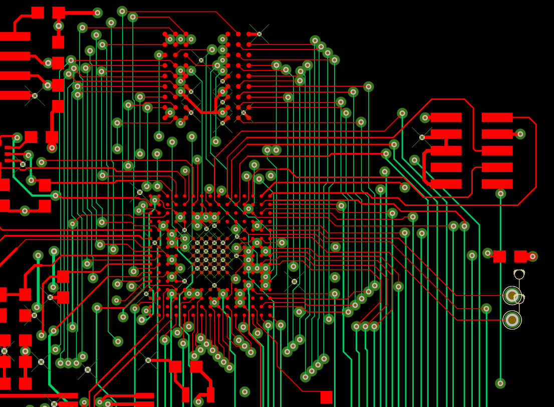
- Group components logically: Place high-speed signals together, isolating analog from digital sections. Position connectors at board edges for easy access.
- Minimize loop areas: Route critical signals with short paths, avoiding right angles that cause reflections.
- Consider thermal hotspots: Space heat-generating parts away from sensitive analog circuits. Provide adequate airflow paths.
- Validate footprints: Ensure pad sizes match component leads, with sufficient solder fillet areas.
Routing and Interconnect Verification
- Follow length-matching rules: Tune differential pairs and clocks to within tolerances for skew control.
- Avoid via farms: Limit vias under components to prevent drill misalignment. Use staggered patterns for dense areas.
- Check power integrity: Split planes only where necessary, bridging with wide traces. Verify stitching vias around cutouts.
- Inspect ground planes: Fill unused areas solidly, removing acute angles that trap etchant.
Per IPC-2221C guidelines, trace dimensions must support anticipated currents without exceeding temperature rise limits. This standard outlines generic requirements for printed board design, aiding in robust layouts.
Design Rule Check (DRC) and Simulation
- Run automated DRC: Flag violations in clearances, widths, and overlaps. Manually inspect high-risk nets.
- Perform signal integrity analysis: Simulate impedance, crosstalk, and eye diagrams for high-speed interfaces.
- Thermal modeling: Predict junction temperatures under load, adjusting vias or planes as needed.
- EMI/EMC review: Ensure guard traces and shielding meet regulatory intent.
DFM and DFA Review
- Panelization assessment: Confirm scoring or tabbing suits volume production. Avoid sharp corners on outlines.
- Solder mask and silkscreen check: Overlap pads adequately without bridging risks. Reference designators clear and oriented consistently.
- Test point placement: Dedicate pads for ICT or flying probe, spaced for probe compatibility.
- Fabrication notes: Specify finishes, tolerances, and special processes like edge plating.
Common Rigid PCB Design Errors and How to Avoid Them
Rigid PCB design mistakes often stem from rushed layouts or overlooked interactions. One frequent issue involves insufficient annular rings around vias, leading to breakout during drilling. To avoid this, enforce rules ensuring copper surrounds holes adequately on all layers. Another error is uneven copper distribution causing warpage; balance pours symmetrically across the board.
Trace necking under components creates high-resistance bottlenecks. Maintain uniform widths through pads and transitions. Improper via back-drilling leaves stubs that degrade high-frequency signals; specify depths precisely in notes. Power plane splits without stitching invite ground bounce; add vias densely along boundaries.
Component shadowing occurs when tall parts block solder wave flow. Elevate or reposition them strategically. Ignoring pad relief in vias traps solder during reflow. Apply tenting where appropriate.
These rigid PCB design errors highlight the need for iterative reviews. Integrating a checklist mitigates them systematically.
Rigid PCB Design Validation and Verification Best Practices
Validation extends beyond DRC to holistic checks. Export Gerber and drill files for third-party review, confirming layer alignment. Simulate assembly with 3D models to spot interference. Prototype a small panel for empirical validation of warpage and bow.
IPC-6012F specifies qualification criteria for rigid boards, including performance under thermal cycling and vibration. Use it to benchmark designs against class requirements. Verification includes electrical testing post-fab, measuring continuity and isolation.
Document deviations with rationale, maintaining traceability. This process solidifies rigid PCB design verification as a core competency.
Conclusion
A thorough rigid PCB design checklist empowers engineers to deliver boards free of costly flaws. By addressing pre-layout planning, routing precision, and validation rigor, teams minimize risks and enhance reliability. Embrace structured reviews to sidestep common pitfalls, ensuring first-pass success. Apply these insights consistently for superior outcomes in every project.
FAQs
Q1: What are the most critical steps in a rigid PCB design checklist?
A1: The rigid PCB design checklist starts with schematic validation, followed by component placement optimization and trace routing per design rules. Post-layout DRC, signal simulation, and DFM review catch remaining issues. Prioritize power integrity and thermal checks to prevent failures. This logical sequence, aligned with engineering standards, ensures comprehensive coverage without omissions.
Q2: How can engineers avoid common rigid PCB design mistakes?
A2: Focus on annular ring adequacy, balanced copper distribution, and via placement to sidestep rigid PCB design errors like breakout or warpage. Use automated tools for DRC alongside manual inspections of high-risk areas. Incorporate iterative simulations for signal and thermal performance. Regular peer reviews add another layer of defense, promoting flawless rigid PCB design review.
Q3: Why is rigid PCB design validation essential before manufacturing?
A3: Rigid PCB design validation confirms compliance with electrical, mechanical, and thermal requirements, preventing scrap from undetected flaws. It includes Gerber checks, 3D assembly models, and prototype testing. This step verifies manufacturability, reducing respin costs. For electric engineers, it guarantees boards meet operational specs under real-world stresses.
Q4: What role do standards play in rigid PCB design verification?
A4: Standards provide benchmarks for trace sizing, clearances, and performance, as in IPC guidelines. They guide rigid PCB design verification by defining class-specific tolerances. Engineers reference them during reviews to ensure reliability. Consistent application minimizes variability and supports qualification testing.
References
- IPC-2221C — Generic Standard on Printed Board Design. IPC, 2023
- IPC-6012F — Qualification and Performance Specification for Rigid Printed Boards. IPC, 2023
- IPC-A-600K — Acceptability of Printed Boards. IPC, 2020


