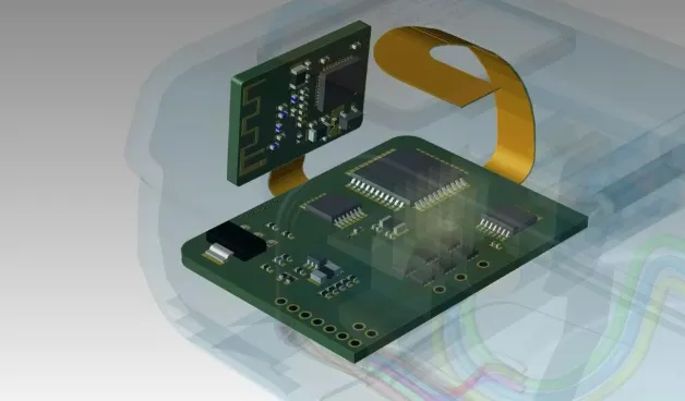
In the contemporary landscape of electronic engineering, the pressure to innovate is relentless. Devices are becoming smaller, more powerful, and increasingly portable, forcing designers to rethink traditional connectivity. While standard rigid PCBs and flexible circuits have served the industry well for decades, the advent of Rigid-Flex PCB Design has revolutionized the way we approach three-dimensional (3D) packaging.
By seamlessly integrating rigid board sections with flexible interconnects into a single unified structure, rigid-flex technology eliminates the need for bulky connectors, reduces system weight, and enhances signal integrity. However, the complexity of a rigid-flex system is significantly higher than its predecessors. Success requires a multidisciplinary approach that blends electrical precision with mechanical durability and material science. This guide explores every critical facet of the rigid-flex design journey.
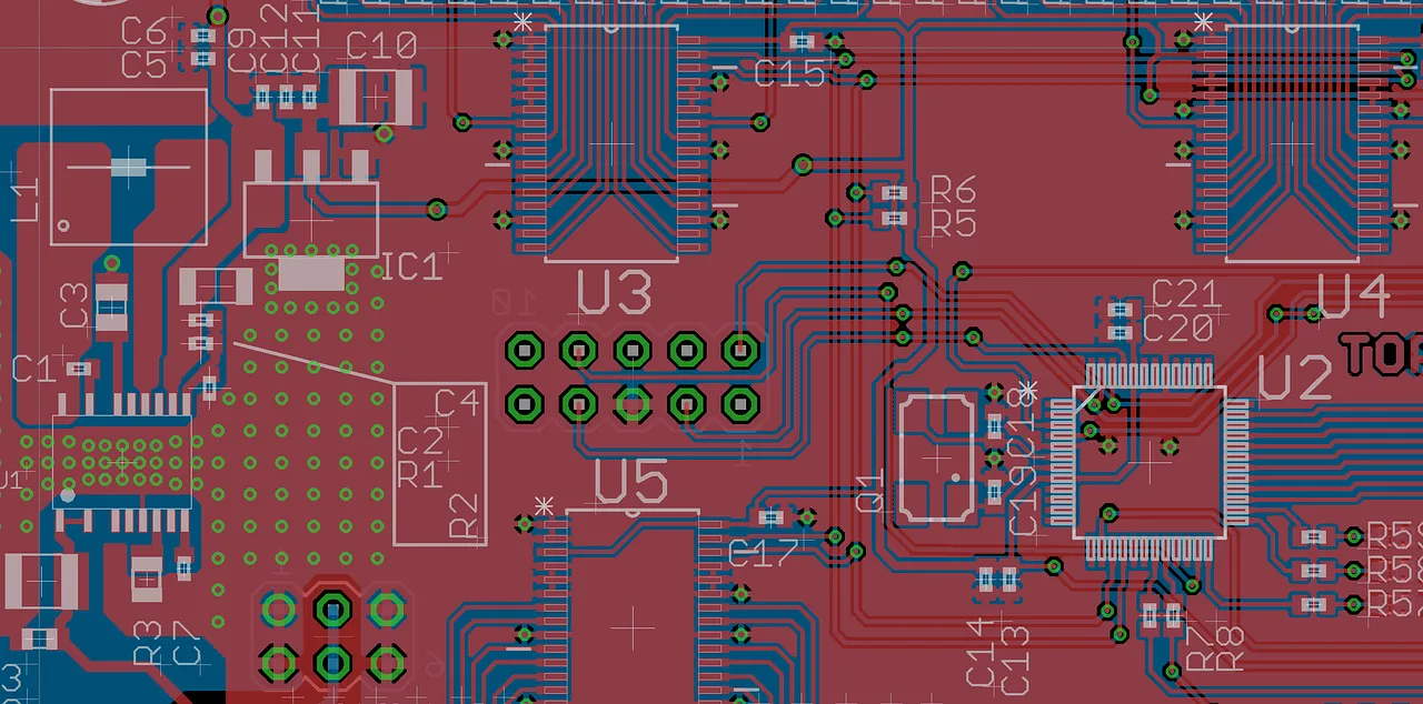
1. The Architectural Blueprint: Mastering the Stack-up
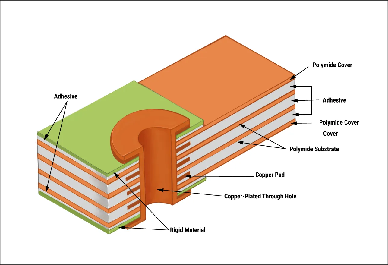
The foundation of any high-performance Rigid-Flex PCB Design is the stack-up. Unlike a standard multilayer board, a rigid-flex stack-up is a hybrid assembly of disparate materials—typically FR4 for the rigid zones and Polyimide (PI) for the flexible zones. Because these materials possess different Coefficients of Thermal Expansion (CTE), the assembly is prone to internal stress during lamination and soldering.
The Importance of Symmetry
Symmetry is the golden rule of stack-up design. An asymmetrical stack-up is the leading cause of board warpage, which can lead to assembly failures and long-term mechanical instability. Designers must ensure that copper weights, dielectric thicknesses, and layer counts are balanced relative to the central flexible core. This "mirrored" approach ensures that the forces exerted during thermal cycles are distributed evenly, keeping the board flat.
Specialized Materials: Adhesiveless and No-Flow Prepreg
Modern designs have largely transitioned to adhesiveless laminates. By removing the acrylic adhesive layer between the copper and the polyimide, the flex section becomes thinner and more thermally stable. Furthermore, in the rigid-to-flex transition zones, designers must use "no-flow" or "low-flow" prepregs. These materials are engineered to stay in place during the high-pressure lamination process, preventing resin from bleeding onto the flexible "wings" and compromising their bendability. To establish a robust structural foundation, engineers should implement 4 pro tips for rigid-flex PCB stack-up design, which provides a strategic framework for mastering layer balance and material symmetry to ensure long-term reliability.
2. Mechanical Integrity: The Science of the Bend Radius
The defining characteristic of a rigid-flex board is its ability to fold. However, copper is a metal, and like all metals, it is subject to work-hardening and fatigue. If a flexible section is bent too sharply or too frequently, the copper traces will develop microscopic cracks, leading to intermittent signals or total failure. This makes Bend Radius the most critical mechanical calculation in the design process.
Static vs. Dynamic Bending
Designers must first categorize the application:
-
Static (Flex-to-Install): The board is folded once to fit inside a chassis. The mechanical stress is constant but non-repeating.
-
Dynamic Flex: The board moves continuously during operation (e.g., a flip-phone hinge or a disk drive head). This requires a much larger bend radius and specialized Rolled Annealed (RA) copper, which has a grain structure better suited for repetitive motion.
Calculating the Safety Margin
The standard industry recommendation for a static bend is a radius at least 10 times the thickness of the flexible laminate. For dynamic applications, this increases to 20 or even 40 times. Failure to adhere to these ratios results in "copper stretching," where the outer traces of a bend are pulled beyond their elastic limit. Deeply understanding the impact of bend radius on rigid-flex PCB reliability is essential for mitigating mechanical stress and copper fatigue, especially in high-reliability sectors like medical and aerospace.
Practical Layout Strategies for Bending
Beyond the raw math, the physical layout of the traces determines success. Traces should cross the bend line at a 90-degree angle. If multiple layers of flex are used, traces should be staggered (staggered layer-to-layer) to avoid the "I-Beam effect," which makes the flex section excessively stiff and prone to cracking. For engineers moving into the execution phase, our practical guide for reliable designs offers a comprehensive look at mastering rigid-flex PCB bend radius through proven formulas and 3D layout techniques.
3. Reliability at the Micro-Scale: Optimizing Via Design
Vias are the electrical "elevators" of a PCB, but in a rigid-flex environment, they are vulnerable. The flexible polyimide core has a significantly higher CTE in the Z-axis (vertical) than the surrounding FR4. During the extreme heat of lead-free soldering, the polyimide expands vertically, exerting massive pressure on the copper barrels of the vias.
Via Placement and Reinforcement
Vias should never be placed in a flexible section that is intended to bend. The rigid via barrel acts as a "stress riser," and the surrounding flex will naturally want to hinge at that point, leading to a snap. Vias should be kept at least 50 mils away from the rigid-to-flex transition line.
To prevent via cracking, designers often use teardrops. By adding a small "fillet" of copper where the trace meets the via pad, the connection is mechanically reinforced. Additionally, using "anchoring spurs"—small extensions of copper that sit under the coverlay—can prevent the via pad from delaminating from the flexible substrate. Ensuring robust connectivity requires optimizing via design in rigid-flex PCBs, a critical step in enhancing electrical and mechanical performance through advanced plating and layout protection.
4. Connectivity: Beyond the Integrated Flex
While the primary goal of Rigid-Flex PCB Design is to minimize external connectors, most systems still require interfaces for modularity, power inputs, or peripheral attachments. The choice of a connector for a flexible substrate is a high-stakes decision.
Stiffeners and Interface Stability
Flexible circuits are too thin to support the weight or the insertion force of most connectors. Therefore, designers must use stiffeners. A stiffener is a piece of FR4 or Polyimide bonded to the back of the flex section to create a localized rigid area. This prevents the connector pins from "peeling" the pads off the flex during mating.
When selecting connectors—such as ZIF (Zero Insertion Force) or board-to-board headers—one must account for the thickness of the flex and the tolerance of the stiffener. If the stiffener is even slightly out of spec, the connector may fail to lock, leading to high contact resistance. For systems requiring external ports, selecting the right connectors for rigid-flex PCBs acts as a comprehensive guide to ensuring interface stability and protecting signal integrity at the physical junction.
5. Economic Engineering: Cost-Effective Design for Manufacturing (DFM)
There is a common misconception that rigid-flex PCBs are prohibitively expensive. While the fabrication cost per square inch is higher than standard PCBs, a holistic view of the system often reveals a lower Total Cost of Ownership (TCO). By removing connectors, cables, and manual assembly labor, rigid-flex can be the more economical choice for complex systems.
Reducing Manufacturing Waste
The cost of rigid-flex is primarily driven by the expensive polyimide materials and the low yield associated with complex lamination. Designers can drive down costs by:
-
Panelization Optimization: Work with your fabricator to ensure the boards are nested on the production panel with minimal waste.
-
Layer Count Control: Avoid adding extra flex layers unless absolutely necessary.
-
Standardizing Transition Zones: Using uniform transition areas simplifies the laser routing process, reducing machine time and cost. Financial success in high-tech projects is achieved by following the cost-effective guide to rigid-flex PCB design, which provides actionable strategies for optimizing materials and manufacturing processes.
6. Advanced Signal Integrity: Impedance in a Hybrid World
Maintaining signal integrity across a rigid-flex boundary is a unique challenge. FR4 and Polyimide have different dielectric constants (Dk). When a high-speed signal travels from the rigid section into the flex section, it encounters a change in the electromagnetic environment, leading to impedance mismatches and signal reflections.
Cross-Hatched Ground Planes
In the flexible section, designers often use a cross-hatched ground plane instead of a solid copper plane. A solid plane makes the flex section very stiff (like a tape measure). A hatched plane provides the necessary ground return path for high-speed signals while allowing the polyimide to remain supple. However, this hatching changes the characteristic impedance of the traces, requiring sophisticated 3D field solvers to calculate the correct trace width.
Transition Zone Routing
To minimize EMI and crosstalk, signals should be routed as differential pairs whenever possible. In the transition zone—where the rigid board meets the flex—traces should be widened slightly to account for the lack of a consistent reference plane during the material crossover.
7. The Material Science: Adhesiveless Polyimide and RA Copper
The choice of materials is where Rigid-Flex PCB Design meets chemistry.
-
Polyimide (PI): Known for its incredible thermal stability, PI can withstand the heat of multiple reflow cycles. It is also inherently flame retardant.
-
Rolled Annealed (RA) Copper: Created by running copper through high-pressure rollers, RA copper has a long, horizontal grain structure. This makes it far superior for bending compared to Electro-Deposited (ED) copper, which has a vertical grain that snaps easily under tension.
-
Coverlay: Instead of a liquid solder mask, flexible circuits use a "Coverlay"—a sheet of polyimide with an adhesive backing. It provides much better protection against moisture and cracking in dynamic applications.
8. Manufacturing Challenges: Plasma Etching and Lamination
Manufacturing a rigid-flex board is a multi-stage process that requires extreme precision.
-
Drilling and Desmearing: When a hole is drilled through a stack of FR4 and PI, the heat can cause the resin to melt and "smear" over the inner copper layers. Standard chemical desmearing is often ineffective on polyimide, so manufacturers must use Plasma Etching to clean the holes and ensure a reliable copper-to-copper bond.
-
Vacuum Lamination: Because the flex sections are often not supported by prepreg (to allow them to stay flexible), the lamination process must use specialized "book" constructions and vacuum presses to prevent air bubbles from being trapped inside the board.
9. Common Mistakes to Avoid in Rigid-Flex Design
Even experienced designers can fall into traps when transition to rigid-flex:
-
Placing Vias on the Bend Line: This is the #1 cause of field failures.
-
Inadequate Stiffeners: Connectors will eventually break the traces if they aren't backed by a stiffener.
-
Ignoring the "Bikini" Cut: This is a manufacturing technique where the coverlay is only applied to the flex section. If the coverlay extends too far into the rigid section, it can cause delamination during assembly.
-
Sharp Trace Angles: Always use curves. 45-degree angles are "stress concentrators."
10. Conclusion: The Strategic Future of Rigid-Flex
Rigid-Flex PCB Design is no longer a niche technology reserved for the military. It is a critical enabler for the next generation of IoT devices, high-speed telecommunications, and life-saving medical electronics.
By mastering the intricacies of stack-up symmetry, calculating precise bend radii, and optimizing via and connector reliability, engineers can create products that are lighter, more durable, and more reliable than ever before. While the initial design curve is steep, the benefits of 3D electronic packaging—and the ability to achieve a cost-effective high-yield production—make rigid-flex the ultimate solution for modern complex systems.
FAQs
Q1: Why are cross-hatched ground planes used instead of solid copper?
A1: Solid copper planes significantly increase the stiffness of the flexible circuit, making it brittle and difficult to bend. Cross-hatching provides a balance between electrical performance (shielding and ground return) and mechanical flexibility, ensuring the board can fold without cracking.
Q2: Is it possible to use standard FR4 solder mask on the flexible portion?
A2: No. Standard solder mask is brittle. If applied to a flexible substrate, it will crack and flake off the moment the board is bent. Flexible circuits must use a "Coverlay" (a polyimide sheet) or a specialized flexible liquid photoimageable (LPI) solder mask.
Q3: How do I determine if my bend is static or dynamic?
A3: If the flexible portion of the PCB only bends during the final assembly of the product and then remains in a fixed position, it is a static bend. If the flex section is expected to move during the product's actual use—such as in a printer head or a wearable joint—it is a dynamic bend and requires more stringent design rules and RA copper.