Introduction
Printed circuit boards face escalating thermal challenges as electronic devices pack more power into smaller spaces. Components like power amplifiers, LEDs, and microcontrollers generate significant heat that can degrade performance, shorten lifespan, or cause outright failure if not managed properly. Effective PCB copper pour thermal management emerges as a critical design strategy to distribute this heat evenly across the board. Copper pour involves filling open areas on PCB layers with solid copper polygons, typically tied to ground or power planes, which leverage copper's superior thermal conductivity to act as heat spreaders. This approach not only improves overall heat dissipation but also integrates seamlessly with other techniques like thermal vias for multilayer boards. For electric engineers designing high-power PCBs, understanding copper pour layout optimizes reliability while adhering to industry design principles.
The relevance of copper pour heat dissipation grows with the rise of applications in automotive electronics, industrial controls, and telecommunications, where operating temperatures often exceed 85 degrees Celsius. Without adequate thermal paths, localized hotspots form around high-power components, leading to issues like delamination or solder joint fatigue. Copper pour mitigates these risks by providing a low-impedance thermal pathway that conducts heat away from critical areas toward board edges or heatsinks. Engineers must consider factors such as board thickness, copper weight, and airflow when implementing these layouts. This article delves into the mechanisms, best practices, and integration strategies for copper pour in thermal management, equipping designers with actionable insights for robust PCB solutions.
What Is Copper Pour and Why It Matters for Thermal Management
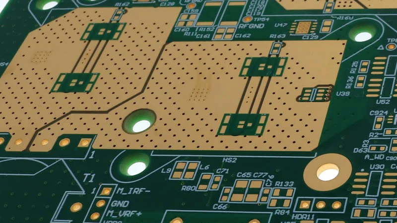
Copper pour refers to the process of flooding unoccupied regions on a PCB layer with a continuous copper area, often connected to a reference plane like ground or voltage supply. This technique transforms otherwise unused space into a functional thermal mass that absorbs, spreads, and dissipates heat from nearby components. In PCB copper pour thermal management, the pour serves as an extension of the heat dissipation network, particularly vital for high-power PCBs where current densities exceed standard trace limits. By increasing the effective surface area exposed to ambient air or forced convection, copper pour enhances natural cooling without additional hardware.
The importance of copper pour heat dissipation becomes evident in scenarios involving power ICs or resistors that dissipate watts of power continuously. Traditional traces alone cannot handle the thermal load efficiently due to their limited cross-section and higher resistance. Pour areas, with their broad geometry, reduce thermal resistance between the heat source and cooler board regions, promoting uniform temperature distribution. This uniformity prevents thermal gradients that could warp the board or stress vias during operation. For electric engineers, incorporating copper pour aligns with design goals for longevity and compliance with performance specifications.
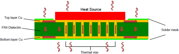
Moreover, in multilayer stacks, copper pours on inner layers contribute to vertical heat transfer when paired with vias. Neglecting pour optimization leads to inefficient designs that rely on oversized heatsinks or fans, increasing system cost and complexity. Proper implementation ensures the PCB itself handles a larger share of thermal duty, making it indispensable for compact, high-reliability electronics.
Technical Principles Behind Copper Pour Heat Dissipation
Copper's thermal conductivity, far superior to substrate materials like FR-4, forms the foundation of effective heat spreading in pour layouts. Heat generated by a component conducts laterally through the pour following principles of conduction, where the rate depends on the temperature gradient and material properties. A solid copper pour minimizes path lengths for heat flow, lowering the overall thermal impedance from source to sink. This spreading effect dilutes hotspot intensity, allowing convection and radiation from larger areas to dominate dissipation.
In quantitative terms, engineers model pour performance using thermal resistance networks, treating the pour as a distributed heat sink. The thickness of the copper layer, typically 1 oz/ft2 or heavier for high-power applications, directly influences conduction efficiency. Thicker pours offer lower thermal resistance but require careful consideration of plating uniformity during fabrication. Integration with thermal vias copper pour further enhances performance by providing interlayer conduction paths, effectively linking pours across the stackup.
Standards like IPC-2221B provide guidelines for incorporating such features into design workflows, emphasizing balanced electrical and thermal performance. Vias within the pour, drilled and plated with copper barrels, act as thermal columns that bridge layers, with array density determining vertical conductance. Engineers calculate via thermal resistance based on diameter, length, and plating thickness, ensuring the pour-via system meets dissipation needs. Radiation from the pour surface contributes marginally but aids in total heat rejection, especially under forced airflow.
Best Practices for Implementing Copper Pour in High-Power PCBs
Start copper pour layout by identifying heat-generating components and surrounding them with contiguous pour areas on all accessible layers. Connect the pour to component pads via short, wide traces or direct stitching to minimize thermal bottlenecks. For copper pour for high-power PCBs, select heavier copper weights, such as 2 oz/ft2 or more, to boost cross-sectional area and reduce temperature rise. Avoid narrow necks or splits in the pour that could create high-resistance zones, as these impede uniform spreading.
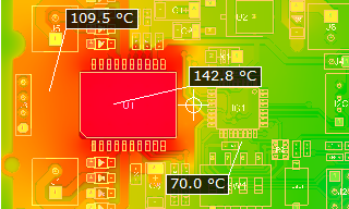
Incorporate thermal vias copper pour strategically under or adjacent to power pads, using arrays of 0.3 mm to 0.5 mm diameter vias spaced at 1 mm pitch for optimal density without compromising structural integrity. Fill and cap vias where possible to enhance conductance and prevent solder wicking during assembly. Maintain pour-to-pour spacing greater than 0.2 mm to allow for fabrication tolerances and prevent shorting. Electric engineers should perform iterative thermal simulations during layout to verify junction temperatures stay below component ratings.
Adhere to IPC-2152 principles for sizing pours analogous to traces, derating for elevated ambient temperatures and multilayer effects. Ground pours benefit from stitching vias around the board perimeter to equalize potentials and aid heat flow to chassis grounds. In designs with exposed pads, tenting the pour selectively preserves solderability while maximizing exposed copper for convection. Testing prototypes with thermocouples validates modeled performance, allowing refinements before production.
Troubleshooting Common Issues in Copper Pour Thermal Management
Engineers often encounter hotspots persisting despite pours due to disconnected islands formed by routing errors or clearance violations. Inspect Gerber files for pour integrity, ensuring nets connect fully without orphans. Another pitfall involves over-reliance on inner-layer pours without adequate surface exposure, where heat traps occur if outer layers lack dissipation paths. Balance stackup by mirroring pours top-to-bottom and verifying via chaining.
Fabrication variations, such as uneven etch depths, can degrade pour effectiveness, particularly in high-current zones. Specify etch compensation in fab notes and review cross-sections post-prototype. In high-power PCBs, electromigration accelerates under combined thermal-electrical stress, so monitor current densities per IPC-2221B limits. Airflow shadows from tall components over pours reduce convection; reposition or add cutouts to channel flow.
Advanced troubleshooting employs finite element analysis to isolate pour contributions, revealing sensitivities to board size or material. For reflow processes, ensure pours do not exacerbate warpage by asymmetrically distributing copper mass. These insights refine designs iteratively, enhancing reliability across production runs.
Conclusion
Copper pour layout stands as a cornerstone of PCB copper pour thermal management, transforming passive board areas into active heat dissipators. By spreading heat through high-conductivity planes and vias, it addresses the core challenges of high-power electronics, ensuring stable operation under demanding conditions. Electric engineers benefit from structured implementation, from pour sizing to via integration, guided by established standards. Prioritizing these practices yields PCBs with superior thermal performance, reduced failure risks, and optimized system integration. As power densities continue rising, mastering copper pour heat dissipation remains essential for innovative designs.
FAQs
Q1: What role does PCB copper pour thermal management play in preventing component failure?
A1: Copper pour enhances heat dissipation by providing a large thermal mass around heat sources, spreading localized heat to reduce peak temperatures. This lowers risks of thermal runaway, electromigration, and solder degradation in high-power components. Paired with thermal vias, it ensures multilayer conduction, aligning with design standards for reliable operation. Engineers achieve this through contiguous pours connected directly to pads.
Q2: How do thermal vias integrate with copper pour for better heat dissipation?
A2: Thermal vias copper pour create vertical pathways linking pours across layers, minimizing interlayer thermal resistance. Arrays under power components conduct heat efficiently, with plating thickness critical for performance. Best placement avoids signal interference while maximizing density. This setup is vital for high-power PCBs, distributing heat uniformly to surfaces for convection.
Q3: When should engineers use copper pour for high-power PCBs?
A3: Opt for copper pour in designs exceeding 1A per square millimeter or with components dissipating over 1W, where trace heating demands spreading. It excels in dense layouts lacking space for discrete heatsinks. Combine with heavier copper layers for demanding environments like automotive or industrial use. Validation through simulation confirms efficacy before fabrication.
Q4: What are key mistakes to avoid in copper pour heat dissipation layouts?
A4: Common errors include isolated pour sections that block heat flow or excessive clearances creating thermal shadows. Neglecting via stitching leads to poor interlayer transfer. Always balance electrical isolation with thermal connectivity, and simulate to catch hotspots early. Adhering to standards prevents these issues in production.
References
IPC-2221B — Generic Standard on Printed Board Design. IPC, 2003
IPC-2152A — Standard for Determining Current Carrying Capacity in Printed Board Design. IPC, 2009
IPC-6012E — Qualification and Performance Specification for Rigid Printed Boards. IPC, 2017


