Introduction
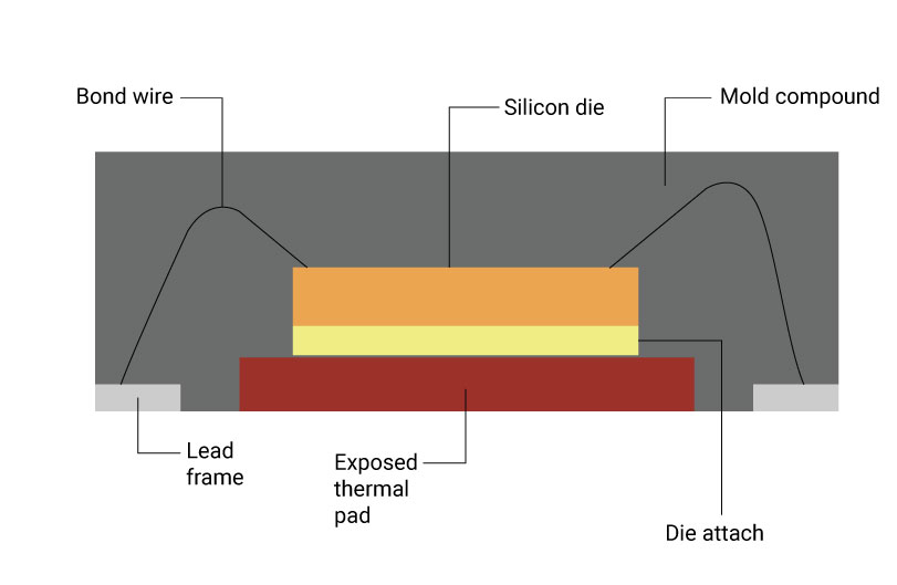
Quad Flat No-lead (QFN) packages have gained widespread use in modern electronics due to their compact size, excellent electrical performance, and superior thermal dissipation capabilities. The exposed thermal pad on the bottom of these packages serves as the primary path for heat transfer to the PCB, making its solder joint integrity crucial for device reliability. However, QFN thermal pad voiding remains a persistent challenge during assembly, often leading to compromised thermal conductivity and potential field failures. Voids form when gases from flux outgassing or solder paste volatilization get trapped under the pad during reflow soldering. This article explores the causes of QFN thermal pad voiding and outlines practical best practices for void reduction, focusing on design, stencil, and process optimizations to enhance QFN assembly reliability.
Engineers designing high-power applications, such as power management ICs or RF modules, must prioritize thermal pad design to minimize these defects. Poor void control not only increases thermal resistance but also accelerates fatigue in the solder joint under thermal cycling. By implementing targeted strategies, assembly yields can improve significantly while meeting industry reliability expectations.
Understanding QFN Thermal Pad Voiding and Its Impact
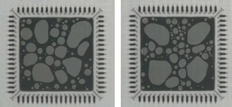
QFN thermal pad voiding refers to the formation of gas pockets or unfilled regions within the solder joint beneath the package's central exposed pad. These voids typically appear as dark spots in X-ray inspections and can occupy varying percentages of the pad area. The primary concern stems from their detrimental effect on heat dissipation, as voids act as insulators, elevating the junction-to-board thermal resistance. In applications demanding high power density, excessive voiding exacerbates hotspot formation and reduces overall system efficiency.
Beyond thermal performance, QFN assembly reliability suffers from void-induced stress concentrations that promote crack propagation during mechanical and thermal stresses. Industry studies show that voiding correlates with higher failure rates in accelerated life tests, underscoring the need for proactive mitigation. Adhering to guidelines in IPC-A-610 ensures acceptable joint quality, where void limits are defined for different classes of assemblies.
Designers often overlook how voiding interacts with other factors like PCB warpage or component standoff, which influence solder flow dynamics. Effective void control directly supports longer service life in automotive, telecommunications, and consumer electronics products.
Related Reading: Beginner's Guide to Thermal Pads: Simple Steps for Effective Heat Dissipation
Root Causes of Thermal Pad Voiding in QFN Assemblies
Several mechanisms contribute to QFN thermal pad voiding, with flux outgassing being the most common culprit. During reflow, volatile components in the solder paste release gases that struggle to escape the confined space under the large thermal pad, leading to entrapment. This effect intensifies with full-area stencil printing, where solder paste covers the entire pad without adequate venting paths.
Thermal vias within the pad exacerbate the issue by wicking molten solder away from the joint, creating starved areas prone to voids. Unplugged vias allow flux residues and gases to migrate upward, further promoting void formation. PCB and package warpage during reflow can also trap air pockets, especially in larger QFN packages where standoff is minimal.
Excessive solder paste volume compounds these problems by generating more gas volume and hindering escape routes. Short reflow profiles fail to allow sufficient preheat for volatilization, while overly aggressive peaks can cause rapid bubbling. Material interactions, such as paste rheology mismatches with lead-free alloys, add variability in production environments.
Related Reading: The Ultimate Guide to Thermal Pad Materials: Choosing the Right One for Your Electronic Project
Optimizing Thermal Pad Pattern Design for QFN Packages
Thermal pad pattern design QFN starts with selecting appropriate land geometries aligned with component datasheets and IPC-7351 standards. This document provides nominal, reduced, and most probable land patterns to balance solder joint strength and reworkability. For QFN packages, the thermal pad land should match the exposed die pad dimensions closely to ensure uniform standoff and minimize fillet excess.
Incorporating venting features into the pattern, such as peripheral channels or subdivided areas, facilitates gas escape during reflow. A common approach divides the pad into smaller rectangles, typically in a 3x5 or 5x5 grid, to create natural bleed-out paths. This design reduces trapped gas while maintaining thermal continuity.
Engineers should verify pattern tolerances using producibility levels outlined in IPC-7351, opting for Level 2 or 3 for high-reliability builds. Simulations of solder volume distribution can predict void risks before prototyping.
Thermal Via Plugging Strategies for QFN Reliability
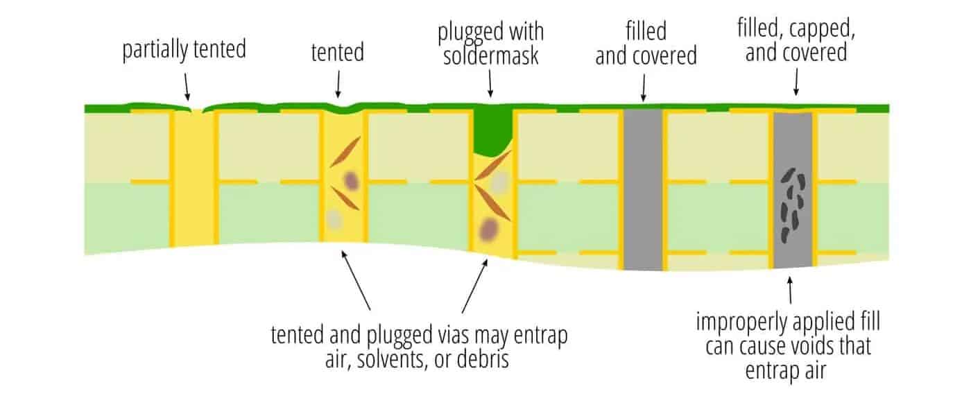
Thermal via plugging QFN is essential to prevent solder loss and void propagation in heat-transfer paths. Vias drilled into the thermal pad enable efficient conduction to inner layers but act as sinks during reflow if left open. Plugging methods include copper plating, epoxy filling, or solder mask tenting to block solder ingress while preserving thermal paths.
Filled vias maintain low thermal impedance comparable to open designs but eliminate wicking. IPC-7095 recommends via-in-pad processes for bottom-terminated components like QFN to control voiding dynamics. Via diameter should be limited to 0.3 mm or smaller, with pitch optimized for density without compromising drill aspect ratios.
In multilayer boards, staggered via arrays enhance spreading while plugged configurations support consistent joint formation. Post-plug planarization ensures flatness for stencil printing.
Controlling Solder Paste Volume for QFN Thermal Pads
Solder paste volume QFN directly influences voiding levels, with optimal coverage around 50 to 80 percent of the pad area proving effective in practice. Full stencil apertures trap gases, whereas reduced openings allow expansion and venting. Stencil thickness typically ranges from 0.1 to 0.125 mm for fine-pitch QFN, paired with laser-cut apertures for precise release.
Window-pane stencil patterns, where openings occupy 60 to 75 percent of the pad via interconnected slots, promote even deposition and flux escape. Type 4 or finer paste particles enhance printability on these features. Printer setup, including squeegee pressure and speed, must align with paste viscosity to avoid bridging or starvation.
Reflow profiling complements volume control, with extended soaks above 150°C promoting outgassing before liquidus.
Assembly Process Best Practices for Void Minimization
Beyond design, QFN assembly reliability hinges on process controls. Nitrogen reflow atmospheres reduce oxidation and void nucleation, particularly for large pads. Vacuum-assisted reflow, though advanced, effectively collapses voids post-liquefaction.
X-ray inspection post-reflow quantifies void percentage, targeting under 25 percent total area per IPC-A-610 Class 3 criteria. Rework challenges arise from voided joints, necessitating precise hot-air profiling and preheating.
Board storage per J-STD-020 prevents moisture-induced voids from popcorning.
Troubleshooting Common QFN Thermal Pad Voiding Issues
When voids persist, start with X-ray analysis to map distribution: central clusters indicate outgassing, peripheral ones suggest via issues. Adjust stencil by increasing opening spacing if coverage exceeds 80 percent. Warpage checks using shadow moire correlate with void hotspots.
Paste formulation tweaks, like low-residue fluxes, address chronic entrapment. Prototype runs validate changes before volume production.
Conclusion
Effective thermal pad design for QFN packages demands integrated attention to land patterns, via plugging, and solder paste management to combat voiding. By following IPC-7351 for patterns, plugging vias per IPC-7095 guidance, and optimizing paste volumes, engineers achieve robust joints with minimal thermal penalties. These practices elevate QFN assembly reliability, ensuring performance in demanding environments. Implementing them systematically reduces defects, cuts rework, and accelerates time-to-market.
FAQs
Q1: How can I reduce QFN thermal pad voiding during assembly?
A1: Target 50 to 80 percent solder paste coverage using window-pane stencil patterns to allow gas venting. Plug thermal vias to prevent wicking, and extend reflow preheat for outgassing. X-ray verification ensures voids stay below acceptability thresholds, enhancing overall QFN assembly reliability.
Q2: What is the best thermal pad pattern design QFN approach?
A2: Follow IPC-7351 land pattern guidelines for optimal pad sizing and tolerances. Incorporate subdivided apertures in stencils for venting while matching package dimensions closely. This balances thermal performance and void control without excessive solder.
Q3: Why is thermal via plugging QFN critical for reliability?
A3: Open vias wick solder from the joint, creating voids and degrading heat transfer. Plugging with epoxy or plating maintains paths while stabilizing standoff. This practice aligns with IPC-7095 for bottom-terminated components, minimizing fatigue risks.
Q4: How does solder paste volume QFN impact void formation?
A4: Excessive volume traps more flux gases under the pad, increasing voids. Reduced coverage via stencil design promotes escape routes during reflow. Fine-tuning to 60 to 75 percent optimizes joint quality and QFN thermal pad voiding control.
References
IPC-7351C — Generic Requirements for Surface Mount Design and Land Pattern Standard. IPC
IPC-7095D — Design and Assembly Process Implementation for Ball Grid Arrays. IPC
IPC-A-610H — Acceptability of Electronic Assemblies. IPC
J-STD-020E — Moisture/Reflow Sensitivity Classification for Nonhermetic Surface Mount Devices. JEDEC


