Introduction
Thermal management in printed circuit board (PCB) design is a critical aspect for ensuring the reliability and performance of electronic devices. As components become smaller and power demands increase, managing heat flow in PCB power distribution systems is essential. Poor thermal design can lead to overheating, component failure, and reduced lifespan of the board. For electronic hobbyists, understanding how to address heat dissipation is vital when designing circuits for personal projects or prototypes. This article explores the principles of thermal PCB design, focusing on heat flow management and power distribution challenges. It provides practical insights into creating efficient designs that maintain optimal temperatures. Whether you are working on a simple LED circuit or a complex power supply, mastering these concepts will improve your project outcomes.
What Is Thermal PCB Design and Why It Matters
Thermal PCB design refers to the process of creating a board layout that effectively manages heat generated by electronic components. It involves strategic placement of parts, selection of materials, and incorporation of heat dissipation techniques to prevent overheating. Heat flow in PCB power distribution is particularly significant because power-intensive components, such as voltage regulators and microcontrollers, generate substantial thermal energy. If not addressed, this energy can cause hotspots, leading to performance issues or permanent damage.
For hobbyists, thermal design matters because it directly impacts the functionality and durability of your creations. A well-designed PCB ensures stable operation even under high loads. It also reduces the risk of thermal stress on components, which can degrade solder joints or warp the board. By prioritizing heat management, you can build more reliable projects that perform consistently over time.
Technical Principles of Heat Flow in PCB Power Distribution
Heat flow in PCB power distribution systems is governed by three primary mechanisms: conduction, convection, and radiation. Conduction transfers heat through the board material and copper traces, making material choice and trace width critical factors. Convection involves heat dissipation into the surrounding air, often aided by airflow or cooling mechanisms. Radiation, though less significant in most cases, refers to heat emitted as infrared energy from hot components.
Power distribution networks on a PCB often involve high current paths, which generate heat due to resistive losses. According to basic electrical principles, heat generation is proportional to the square of the current multiplied by resistance. Therefore, narrow traces or insufficient copper thickness can exacerbate thermal issues. Additionally, components with high power dissipation, like power transistors, act as localized heat sources, creating uneven temperature distribution across the board.
Thermal resistance, a measure of how much a material opposes heat flow, is another key concept. Multilayer PCB, for instance, can reduce thermal resistance by spreading heat across multiple copper layers. Standards such as IPC-2221B, which provides guidelines for PCB design, emphasize the importance of calculating thermal paths to avoid excessive temperature rise. Understanding these principles helps hobbyists anticipate and mitigate potential heat-related problems in their designs.
Practical Solutions for Thermal Management in PCB Design
Managing heat flow in PCB power distribution requires a combination of design techniques and material considerations. Below are actionable strategies tailored for hobbyists working on various projects.
Optimize Component Placement
Place heat-generating components, such as power regulators, away from sensitive parts like microcontrollers. Grouping high-power elements together near heat dissipation features, like board edges, can improve natural convection. Ensure adequate spacing between components to prevent heat buildup in confined areas.
Use Appropriate Trace Widths
Wider copper traces reduce resistance and, consequently, heat generation in power distribution paths. Calculate trace widths based on current requirements using guidelines from standards like IPC-2221B. Heavy copper pcb, often specified in ounces per square foot, also enhance heat conduction away from critical areas.
Incorporate Thermal Vias
Thermal vias are small holes filled or plated with copper that transfer heat between board layers. Place them under or near high-power components to conduct heat to inner or bottom layers for dissipation. Arrays of vias can create efficient thermal paths, especially in multilayer designs.
Select Suitable Board Materials
The substrate material impacts thermal conductivity. Standard FR-4 material has moderate thermal performance, but for high-power applications, consider materials with higher thermal conductivity if budget allows. Check material specifications to ensure they meet thermal requirements without compromising electrical properties.
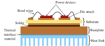
Add Heat Sinks or Cooling Features
For components with significant heat output, attach small heat sinks to draw heat away. Ensure proper mounting and thermal interface material to maximize contact efficiency. In some hobbyist projects, small fans can be integrated for forced convection if natural airflow is insufficient.
Leverage Ground Planes
Solid copper ground planes act as heat spreaders, distributing thermal energy across a larger area. Connect heat-generating components to these planes with thermal vias to enhance dissipation. This technique is particularly effective in managing heat flow in PCB power distribution networks.
Simulate and Test Designs
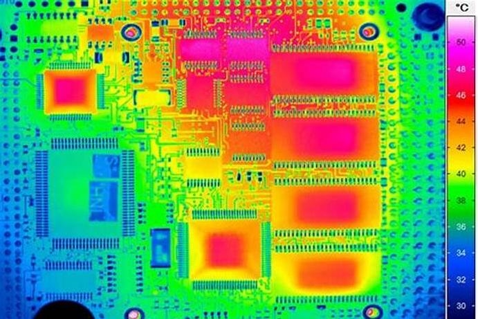
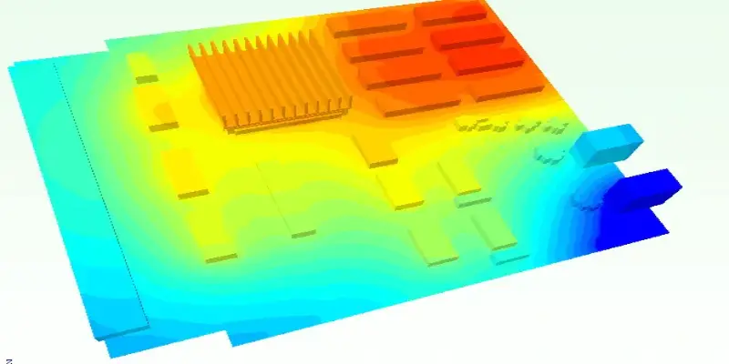
Before finalizing a layout, use thermal simulation tools available in many free or open-source design software packages. These tools predict temperature distribution and identify potential hotspots. After fabrication, test the board under load conditions with a thermal camera or temperature probe to verify performance.
Common Thermal Challenges and Troubleshooting Tips
Hobbyists often encounter thermal issues when scaling up from simple to more complex designs. One common problem is unexpected overheating in power distribution circuits, often due to undersized traces or poor component placement. If a component feels excessively hot to the touch during operation, measure its temperature and compare it against its datasheet limits. Relocate the part or increase trace width if necessary.
Another issue is thermal stress causing board warpage or solder joint failure. Standards like IPC-A-600K outline acceptable limits for board flatness and visual defects. Inspect your PCB for signs of bending after prolonged operation, and consider adding mechanical supports if warpage occurs.
Finally, insufficient heat dissipation in enclosed projects can trap heat. Ensure ventilation holes or slots are present in enclosures to allow airflow. If using a fan is not feasible, consider redesigning the layout to spread heat more evenly across the board surface.
Advanced Considerations for High-Power Designs
For hobbyists venturing into high-power applications, such as motor drivers or power supplies, additional thermal design strategies become relevant. Multilayer boards can significantly improve heat distribution by providing more copper area for heat spreading. Inner layers can serve as dedicated thermal planes connected via thermal vias.
Pay attention to the power dissipation ratings of components, as outlined in their technical documentation. Derating components, or operating them below their maximum capacity, can prevent thermal overload. Standards like IPC-6012E provide performance specifications for rigid boards under thermal stress, offering guidance on ensuring long-term reliability.
Additionally, consider the ambient temperature of your project's operating environment. High ambient conditions reduce the temperature margin for components, necessitating more aggressive cooling solutions. Testing under worst-case scenarios ensures your design can withstand real-world conditions.
Conclusion
Thermal PCB design is a fundamental skill for electronic hobbyists aiming to build reliable and efficient projects. By understanding heat flow in PCB power distribution systems, you can prevent overheating and extend the lifespan of your creations. Implementing strategies like optimized component placement, wider traces, thermal vias, and ground planes significantly improves heat management. Testing and troubleshooting further ensure your design performs as intended. With these principles, you can confidently tackle projects of varying complexity, knowing that thermal challenges are under control. Prioritizing heat dissipation not only enhances performance but also builds your expertise in crafting robust electronic solutions.
FAQs
Q1: How does heat flow affect PCB power distribution performance?
A1: Heat flow in PCB power distribution directly influences performance by impacting component efficiency and reliability. Excessive heat from high-current paths can cause voltage drops or component failure. Proper trace sizing and thermal vias, as guided by standards like IPC-2221B, help manage heat. Monitoring temperature during testing ensures the board operates within safe limits for consistent performance.
Q2: What are simple ways to improve thermal management in PCB design?
A2: Improving thermal management in PCB design involves basic steps like spacing components for airflow, using wider traces for power distribution, and adding thermal vias. Incorporate ground planes to spread heat and attach heat sinks to high-power parts. These methods, aligned with IPC-2221B guidelines, are accessible to hobbyists and significantly reduce overheating risks in small projects.
Q3: Why is thermal design critical for high-power PCB applications?
A3: Thermal design is vital for high-power PCB applications because significant heat generation can damage components or degrade performance. Effective heat flow management in power distribution prevents hotspots and ensures stability. Following standards like IPC-6012E helps maintain board integrity under thermal stress. Proper cooling techniques are essential to handle the increased thermal load in such designs.
References
IPC-2221B — Generic Standard on Printed Board Design. IPC, 2012.
IPC-A-600K — Acceptability of Printed Boards. IPC, 2020.
IPC-6012E — Qualification and Performance Specification for Rigid Printed Boards. IPC, 2020.


